Supercharge Your Innovation With Domain-Expert AI Agents!

Semiconductor structure and formation method thereof

A semiconductor and isolation structure technology, which is applied in the field of semiconductor structure and its formation, can solve the problems such as the electrical performance of semiconductor devices needs to be improved, and achieve the effects of suppressing short channel effects, reducing implantation damage, and less loss of doping ions

Inactive Publication Date: 2018-10-23
SEMICON MFG INT (SHANGHAI) CORP +1
View PDF4 Cites 2 Cited by
  • Summary
  • Abstract
  • Description
  • Claims
  • Application Information

AI Technical Summary

Problems solved by technology

[0004] However, the electrical performance of semiconductor devices formed by the prior art needs to be improved

Method used


Image

  • Semiconductor structure and formation method thereof
  • Semiconductor structure and formation method thereof
  • Semiconductor structure and formation method thereof

Examples


Embodiment Construction

[0015] It can be seen from the background art that the electrical performance of semiconductor devices formed in the prior art needs to be improved. Combining with a method of forming a semiconductor structure, the reason why its electrical performance needs to be improved is analyzed.

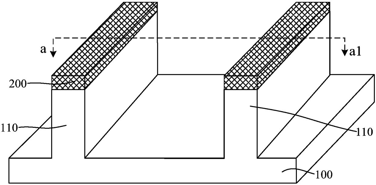
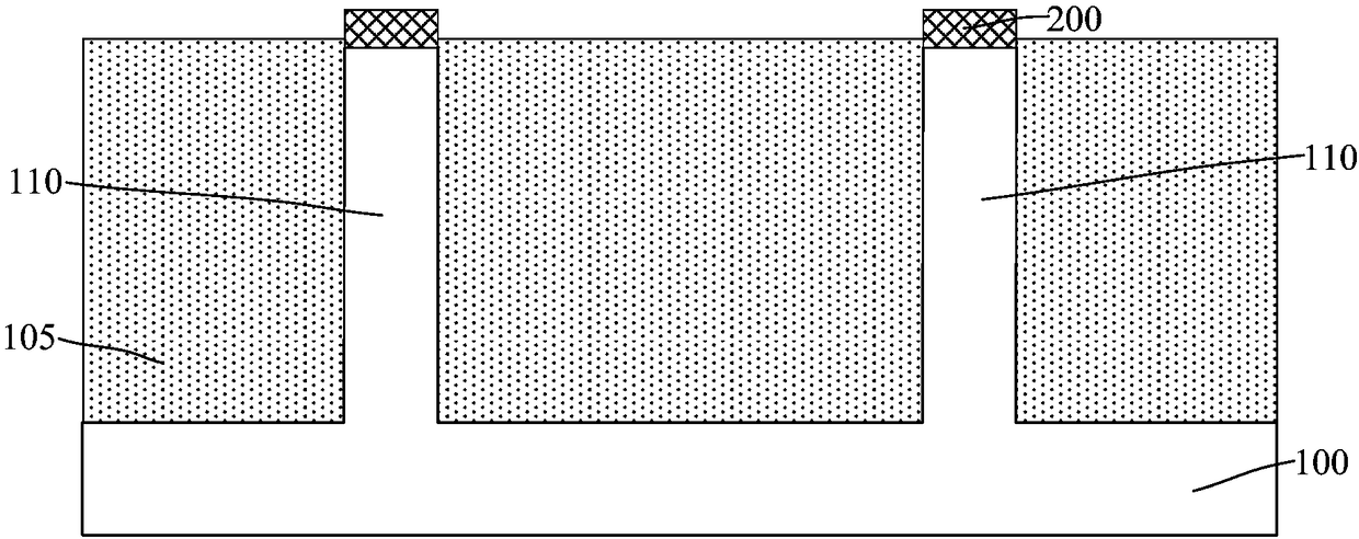
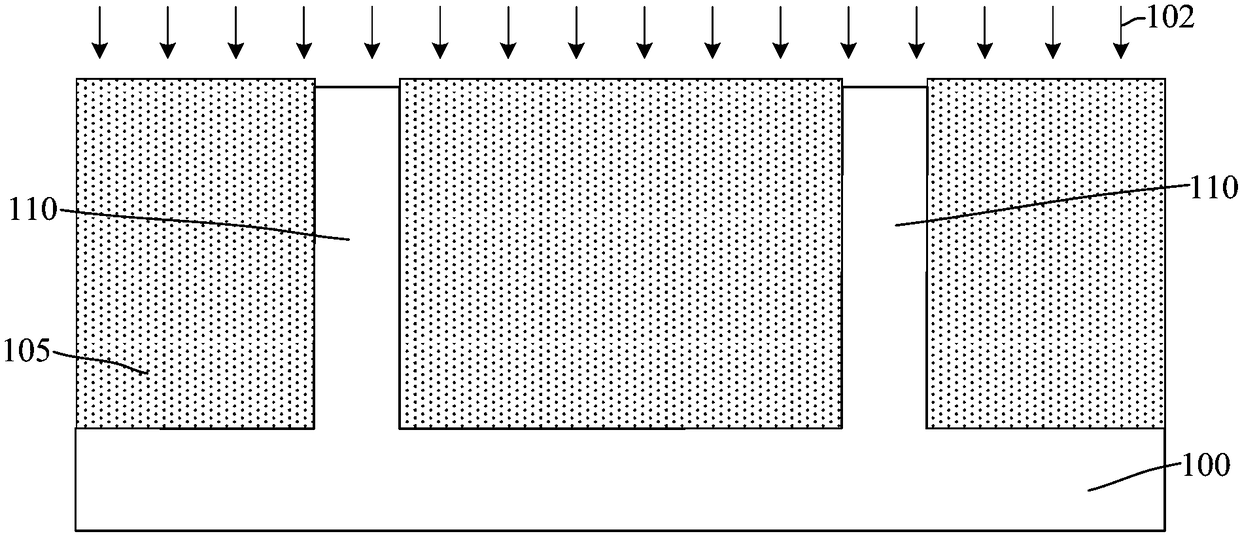
[0016] The forming method includes: providing a base, the base including a substrate and discrete fins located on the substrate; forming an isolation film on the substrate where the fins are exposed, and the isolation film covers the fins After forming the isolation film, perform well implantation (Well Implant) process on the fin; after the well implantation process, perform anti-punch through ion implantation (Anti-punch Through Implant) on the fin process, forming an anti-penetration doping ion region in the fin; etching back a partial thickness of the isolation film, leaving the isolation film as an isolation structure, the isolation structure covering part of the sidewall of the fin, and ...


PUM


Abstract

The invention relates to a semiconductor structure and a formation method thereof. The formation method includes the following steps that: a base is provided, wherein the base comprises a substrate and discrete fins on the substrate; an isolation structure is formed on the substrate which is not covered by the fins, wherein the isolation structure covers partial sidewalls of the fins; a gate structure which spans the fins and cover partial top surfaces and sidewall surfaces of the fins is formed; the fins at two sides of the gate structure are etched by a certain thickness, so that grooves canbe formed in the fins; anti-punch-through ion implantation is performed on the bottoms of the grooves, so that anti-punch-through doped ion regions can be formed in the fins at the bottoms of the grooves; and doped epitaxial layers are formed in the grooves. Compared with an anti-punch-through ion implantation process which is performed before the isolation structure is formed, the anti-punch-through ion implantation process of the formation method of the invention is small in implantation dose, thereby reducing implantation damage to the fins; anti-punch-through ion implantation is performedon the bottoms of the grooves, so that a short channel effect can be suppressed; and therefore, the electrical performance of the formed semiconductor device is improved.

Description

technical field [0001] The invention relates to the field of semiconductor manufacturing, in particular to a semiconductor structure and a forming method thereof. Background technique [0002] In semiconductor manufacturing, with the development trend of VLSI, the feature size of integrated circuits continues to decrease. In order to accommodate the reduction in feature size, the channel length of MOSFETs has also been shortened accordingly. However, as the channel length of the device is shortened, the distance between the source and the drain of the device is also shortened, so the control ability of the gate to the channel becomes worse, and the gate voltage pinches off the channel. The difficulty is also increasing, making the phenomenon of subthreshold leakage (subthreshold leakage), the so-called short-channel effect (SCE: short-channel effects) more likely to occur. [0003] Therefore, in order to better adapt to the reduction of the feature size, the semiconductor ...

Claims


Application Information

Patent Timeline
Patent Type & Authority Applications(China)
IPC IPC(8): H01L21/8234H01L21/8238H01L27/088H01L27/092
CPCH01L21/823431H01L21/823821H01L27/0886H01L27/0924
Inventor 李勇林仰魁
Owner SEMICON MFG INT (SHANGHAI) CORP
Features
  • R&D
  • Intellectual Property
  • Life Sciences
  • Materials
  • Tech Scout
  • Unparalleled Data Quality
  • Higher Quality Content
  • 60% Fewer Hallucinations
Learn More