Method for forming fin field effect transistor
A fin field effect and transistor technology, which is applied in the fields of semiconductor devices, semiconductor/solid-state device manufacturing, electrical components, etc., can solve the problems of poor transistor performance and reliability, avoid etching damage, reduce the degree of etching, and reduce resistance. Effect
- Summary
- Abstract
- Description
- Claims
- Application Information
AI Technical Summary
Problems solved by technology
Method used
Image

Examples
Embodiment Construction
[0032] As the feature size of the fin field effect transistor formed in the prior art is further reduced, the performance and reliability of the fin field effect transistor are poor.
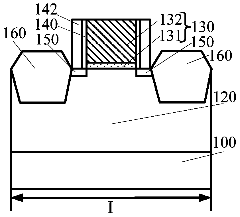
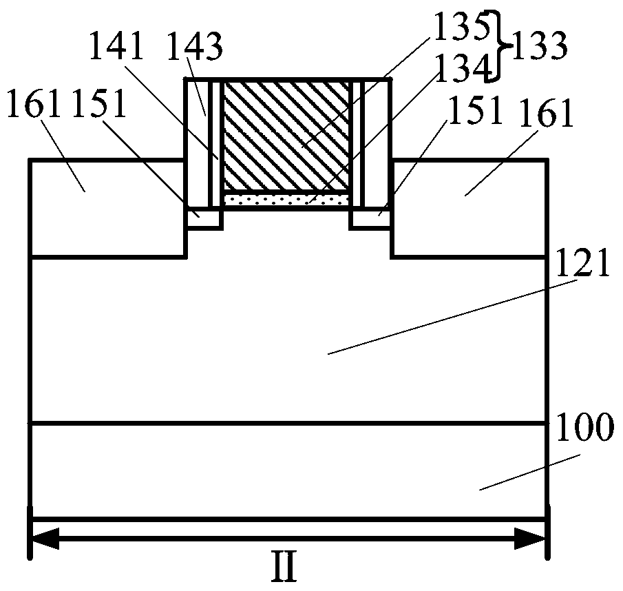
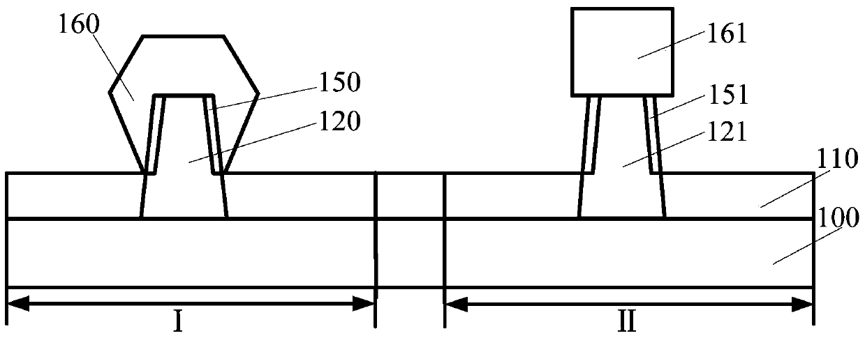
[0033] Figure 1 to Figure 3 It is a schematic diagram of the structure of a fin field effect transistor in an embodiment of the present invention.
[0034] The forming method of the fin field effect transistor comprises the following steps: in combination with reference Figure 1 to Figure 3, providing a semiconductor substrate 100, the semiconductor substrate 100 has a PMOS region (I region) and an NMOS region (II region), the surface of the semiconductor substrate 100 in the PMOS region has a first fin 120 and a first fin 120 across the first fin 120 A gate structure 130, the first gate structure 130 covers part of the top surface and sidewall of the first fin 120; the surface of the semiconductor substrate 100 in the NMOS region has the second fin 121 and the second fin 121 across the second ...
PUM
 Abstract
Description
Claims
Application Information