Method for calculating contact pressure between grinding pad and surface of chip in CMP simulation model

A technology of contact pressure and calculation method, which is applied in the fields of calculation, instrumentation, electrical and digital data processing, etc., can solve the problems of lack of CMP model realization technology, and achieve the effect of generality and versatility, and improving the calculation speed.

Active Publication Date: 2014-09-03
INST OF MICROELECTRONICS CHINESE ACAD OF SCI
View PDF4 Cites 10 Cited by
  • Summary
  • Abstract
  • Description
  • Claims
  • Application Information

AI Technical Summary

Problems solved by technology

[0004] However, in the prior art, the CMP model and implementation technology that can take into account both the grinding mechanism and the calculation efficiency of the contact pressure between the polishing pad and the chip surface are very scarce, resulting in the calculation of the contact pressure between the polishing pad and the chip surface that can take into account both calculation efficiency and accuracy. The study of the method has become an important topic in the process of CMP dynamic simulation

Method used


Image

  • Method for calculating contact pressure between grinding pad and surface of chip in CMP simulation model
  • Method for calculating contact pressure between grinding pad and surface of chip in CMP simulation model
  • Method for calculating contact pressure between grinding pad and surface of chip in CMP simulation model

Examples


Embodiment 1

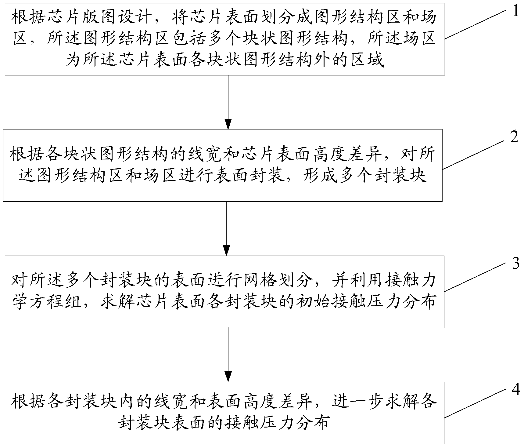
[0065] Such as figure 1 As shown, the embodiment of the present invention provides a calculation method of the contact pressure between the polishing pad and the chip surface in a CMP simulation model, including:

[0066] Step 1: Divide the chip surface into a graphic structure area and a field area according to the chip layout design, the graphic structure area includes a plurality of block graphic structures, and the field area is the area outside each block graphic structure on the chip surface .

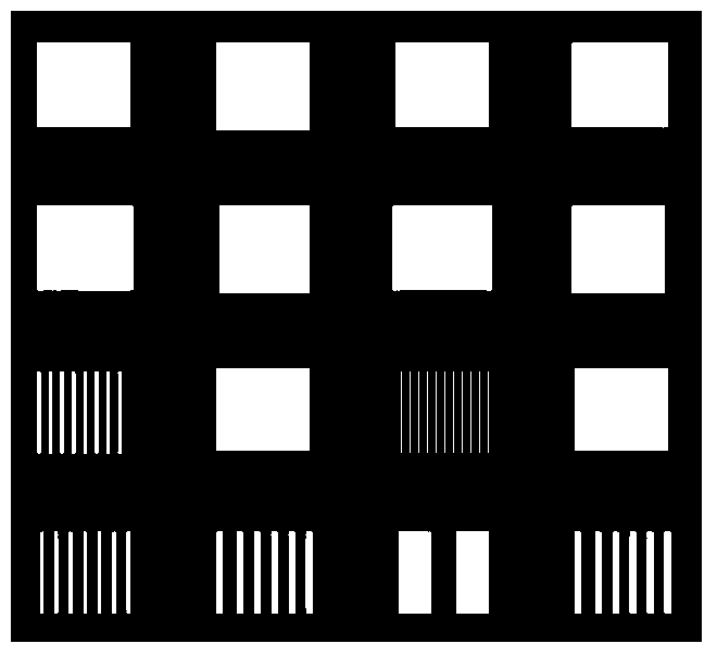
[0067] Take a 2cm*2cm chip as an example, such as figure 2 As shown, according to the chip layout design, the chip surface is divided into a pattern structure area and a field area, and the pattern structure area includes a plurality of block pattern structures, and the field area refers to figure 2 The black area on the surface of the middle chip except for each block pattern structure.

[0068] Step 2: according to the difference in line width and chip surface height of ea...


PUM


Abstract

The embodiment of the invention discloses a method for calculating the contact pressure between a grinding pad and the surface of a chip in a CMP simulation model. The method includes the first step of dividing the surface of the chip into a graph structural region and a field region according to the layout design of the chip, wherein the graph structural region comprises multiple block graph structures, and the field region is the region in the surface of the chip except all the block graph structures, the second step of conducting surface packaging on the graph structural region and the field region to form multiple package blocks according to line widths of all the graph structures and the height difference of the surface of the chip, the third step of conducting grid division on the surfaces of the multiple package blocks and solving initial contact pressure distribution of each package block on the surface of the chip through a contact mechanic equation set, the fourth step of further solving the contact pressure distribution of the surfaces of all the package blocks according to the widths of lines in the package blocks and the surface height difference of the package blocks. Through the method, the calculation efficiency and calculation accuracy can be achieved simultaneously, so that the method has generality and university.

Description

technical field [0001] The invention relates to the technical fields of manufacturability design and chemical mechanical polishing modeling, in particular to a calculation method for contact pressure between a polishing pad and a chip surface in a CMP simulation model. Background technique [0002] With the continuous expansion of integrated circuit wafer size and the continuous reduction of chip feature size, it is increasingly difficult to control the stability of chips. Many derivative effects are not fully considered before design, and the improvement of integrated circuit yield is significantly affected. Design for Manufacturability (DFM), as a nascent nano-design methodology technology, provides a technical platform covering design and manufacturing information, so that designers can predict the influence of different design schemes in the process manufacturing stage in advance, and optimize the design , further reducing the decrease in chip yield due to design defects...

Claims


Application Information

Patent Timeline
Patent Type & Authority Applications(China)
IPC IPC(8): G06F17/50
Inventor 徐勤志陈岚
Owner INST OF MICROELECTRONICS CHINESE ACAD OF SCI
Why Eureka
Try Eureka