Static memory cell and forming method thereof

A static storage, single technology, used in electrical components, semiconductor/solid-state device manufacturing, electrical solid-state devices and other directions, can solve the problem of SRAM memory performance is not stable enough, to achieve superior performance, stable performance, meet the effect of driving current

Active Publication Date: 2014-09-03
SEMICON MFG INT (SHANGHAI) CORP
View PDF5 Cites 12 Cited by
  • Summary
  • Abstract
  • Description
  • Claims
  • Application Information

AI Technical Summary

Problems solved by technology

[0008] However, as the process node is further reduced, the performance of the SRAM memory formed by the prior art is not stable enough

Method used


Image

  • Static memory cell and forming method thereof
  • Static memory cell and forming method thereof
  • Static memory cell and forming method thereof

Examples


Embodiment Construction

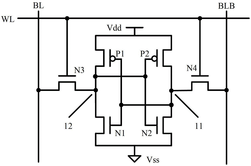
[0037] As mentioned in the background art, the performance of the SRAM memory formed in the prior art is not stable enough.

[0038]After further research, the inventors found that in the storage unit of the SRAM memory, compared with the pull-up transistor (Pull Up Transistor), the pull-down transistor (Pull Down Transistor) generally requires a larger drive current (Drive Current). The performance of the SRAM memory formed in the prior art is not stable enough, the main reason being that the driving current of the pull-down transistor is insufficient.

[0039] After further research, the inventors found that the driving current of the pull-down transistor is largely determined by the effective width of the fin constituting the pull-down transistor. The greater the effective width of the fin constituting the pull-down transistor, the greater the driving current of the formed pull-down transistor. How to increase the effective width of the fin constituting the pull-down trans...


PUM


Abstract

A static memory cell and a forming method thereof are provided; the static memory cell comprises the following elements: a semiconductor substrate comprising a first zone forming a pull down transistor and a second zone forming a pull up transistor; a first pin portion positioned on a surface of the semiconductor substrate in the first zone and a second fin portion positioned on a surface of the semiconductor in the second zone, wherein a top of the second fin portion is provided with an insulation layer; an interlayer medium layer covering the semiconductor substrate surface besides the first fin portion and the second fin portion, and a surface of the interlayer medium layer is lower than a top surface of the first and second fin portions; a first grid electrode structure positioned on the surface of the interlayer medium layer and capable of crossing the top and a side wall of the single first fin portion, and a second grid electrode structure positioned on the surface of the interlayer medium layer and capable of crossing a top and a side wall of the single second fin portion, and the second grid electrode structure is isolated from the top portion of the second fin portion through an insulation layer. The static memory cell is stable in performance, and a finally formed SRAM memory is excellent in performance.

Description

technical field [0001] The present invention relates to the technical field of semiconductor manufacturing, in particular to a static storage unit and a method for forming the same. Background technique [0002] Static Random Access Memory (SRAM), as a member of memory, has the advantages of high speed, low power consumption and compatibility with standard processes, and is widely used in computers, personal communications, consumer electronics (smart cards, digital cameras, Multimedia player) and other fields. [0003] figure 1 It is a schematic diagram of the circuit structure of the storage unit of the existing 6T structure SRAM memory, the storage unit includes: a first PMOS transistor P1, a second PMOS transistor P2, a first NMOS transistor N1, a second NMOS transistor N2, and a third NMOS transistor N3 and a fourth NMOS transistor N4. [0004] The first PMOS transistor P1, the second PMOS transistor P2, the first NMOS transistor N1, and the second NMOS transistor N2...

Claims


Application Information

Patent Timeline
Patent Type & Authority Applications(China)
IPC IPC(8): H01L27/11H01L21/8244
Inventor 洪中山
Owner SEMICON MFG INT (SHANGHAI) CORP
Why Eureka
Try Eureka