Capacitive touching structure, embedded touch screen, display device and scanning method of display device

An embedded touch screen and capacitive technology, which is applied in the fields of electrical digital data processing, optics, instruments, etc., can solve the problems of large touch blind area, unfavorable narrow frame design, and a large number of peripheral traces, etc., to reduce the number of traces , Reduce the effect of relatively large touch blind area and the reduction of the number of wires

Active Publication Date: 2014-09-10
BOE TECH GRP CO LTD +1
View PDF8 Cites 55 Cited by
  • Summary
  • Abstract
  • Description
  • Claims
  • Application Information

AI Technical Summary

Problems solved by technology

[0005] And, in concrete implementation, the quantity of self-capacitance electrode can be very much, be 5mm*5mm as example with the occupied area of ​​each self-capacitance electrode, 5 inches liquid crystal screen just needs 264 self-capacitance electrodes, if each If the self-capacitance electrode design is smaller, there will be more self-capacitance electrodes, so that the number of wires connected to the self-capacitance electrodes is very large, which will cause some problems. There will also be a large number of peripheral traces connected to the...

Method used


Image

  • Capacitive touching structure, embedded touch screen, display device and scanning method of display device
  • Capacitive touching structure, embedded touch screen, display device and scanning method of display device
  • Capacitive touching structure, embedded touch screen, display device and scanning method of display device

Examples


Embodiment 1

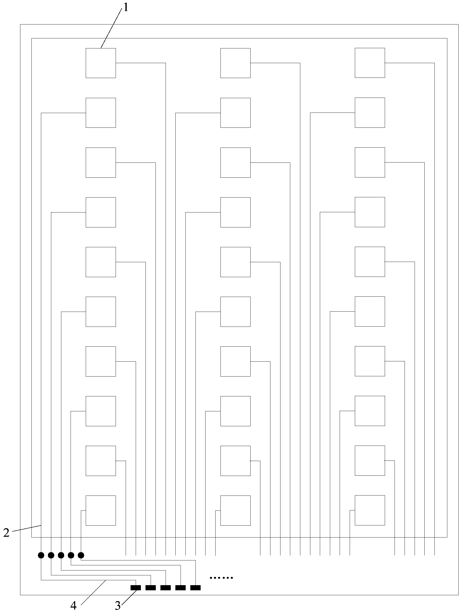
[0165] In the first embodiment of the present invention, the combination of image 3 , the structure of the capacitive touch structure is introduced in detail.

[0166] like image 3 As shown, the capacitive touch structure applied to the touch screen includes:

[0167] A plurality of self-capacitance electrodes 10 arranged on the same layer and insulated from each other in a matrix form are respectively located in the upper and lower regions that are not equally divided along the horizontal direction included on the surface of the film layer where the self-capacitance electrodes 10 are located; in, image 3 The description will be made by taking 16 self-capacitance electrodes 10 in 4 rows and 4 columns in the upper region and 12 self-capacitance electrodes 10 in 3 rows and 4 columns in the lower region;

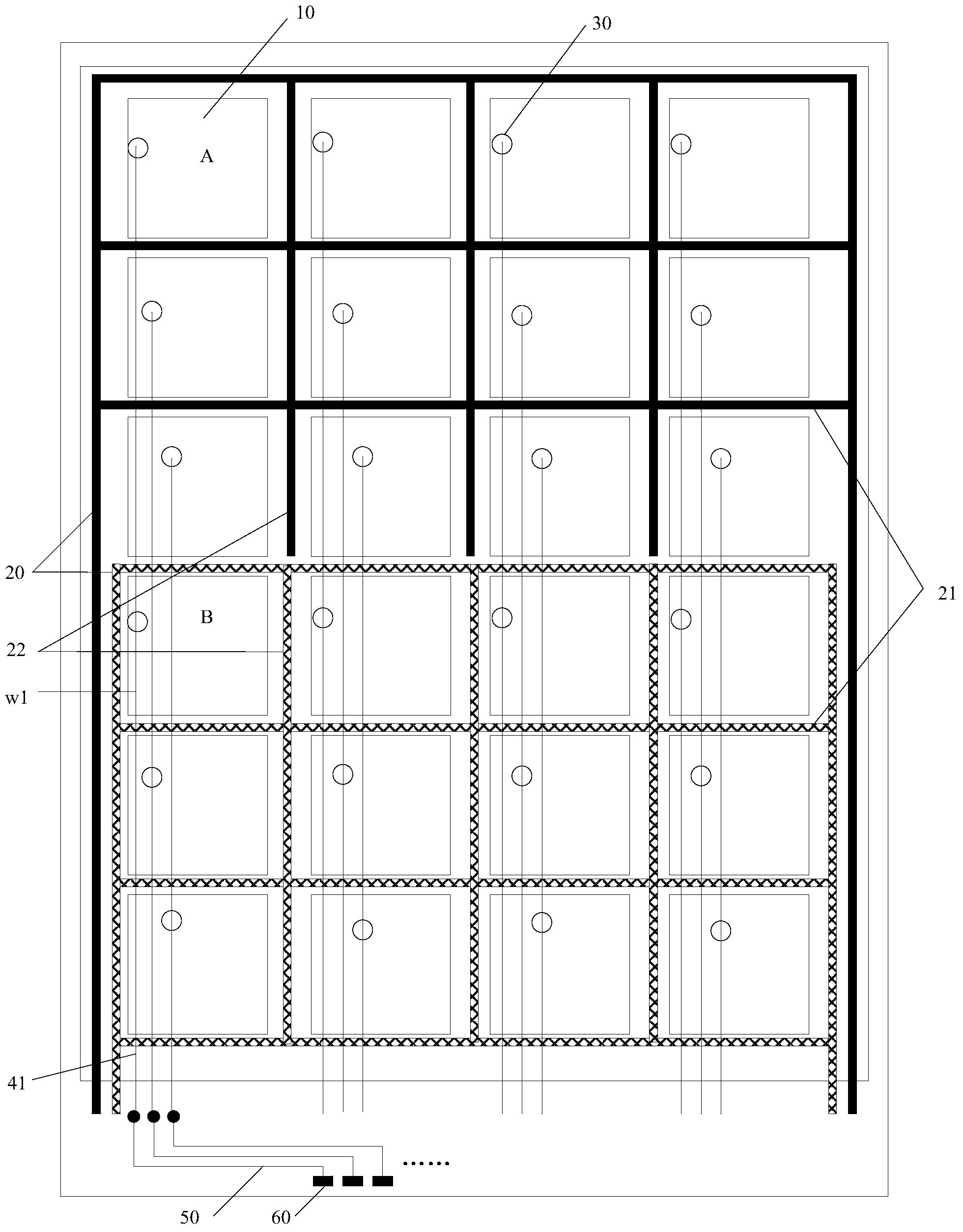
[0168] A regional electrode 20 located in each of the regions, the regional electrode 20 located in the upper region is arranged on the same layer as the self-capacitance...

Embodiment 2

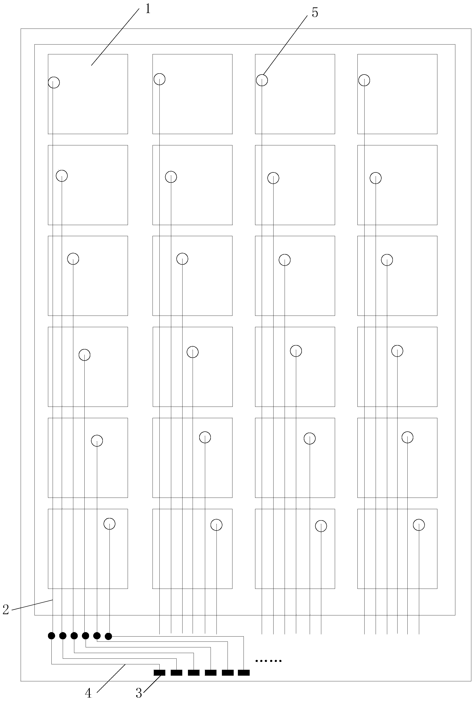
[0178] In the second embodiment of the present invention, the combination of image 3 , the touch principle of the capacitive touch structure applied to the touch screen in the embodiment of the present invention is introduced in detail.

[0179] 1. Single touch.

[0180] 1. The touch point is located at image 3 in the upper region shown.

[0181] Such as Figure 4 shown in the image 3 Point P1 in the upper area shown partially overlaps the regional electrode pad1, self-capacitance electrode A, self-capacitance electrode B, self-capacitance electrode E, and self-capacitance electrode F in the upper area; P1 point overlaps with the self-capacitance electrode The overlapping area of ​​A is S1, the overlapping area of ​​P1 point and self-capacitance electrode B is S4, the overlapping area of ​​P1 point and self-capacitance electrode E is S2, and the overlapping area of ​​P1 point and self-capacitance electrode F The area is S3, where S2>S1>S3>S4;

[0182] when the finger ...


PUM


Abstract

The invention relates to the technical field of touching, in particular to a capacitive touching structure, an embedded touch screen, a display device and a scanning method of the display device. The number of wires in the self-capacitance touching structure is decreased, and the probability of occurrence of the problems that the narrow frame design is not facilitated and a touch blind area is large is decreased to a certain degree. The capacitive touching structure comprises a plurality of self-capacitance electrodes which are arranged on the same layer, area electrodes, first wires, second wires and touch detection chips, wherein the self-capacitance electrodes are located in at least two areas contained by the surface of a film where the self-capacitance electrodes are located respectively; the area electrodes are located in the areas respectively, and the area electrodes and the self-capacitance electrodes are located on the same layer; the first wires are connected with the self-capacitance electrodes, and each first wire is connected with at least two self-capacitance electrodes which are located in different areas respectively; the second wires are connected with the area electrodes, and the area electrodes located in the areas are electrically connected with the different second wires; the touch detection chips are connected with the first wires and the second wires.

Description

technical field [0001] The invention relates to the field of touch technology, in particular to a capacitive touch structure, an embedded touch screen, a display device and a scanning method thereof. Background technique [0002] With the rapid development of display technology, touch screen panels (Touch Screen Panels) have gradually spread in people's lives. At present, the touch structures included in the touch screen can be divided into: a mutual capacitance touch structure and a self-capacitance touch structure. As for the self-capacitance touch structure, due to its high accuracy of touch sensing and relatively high signal-to-noise ratio, it is favored by major panel manufacturers. [0003] At present, the self-capacitance touch structure uses the principle of self-capacitance to detect the touch position of the finger. Specifically, a plurality of self-capacitance electrodes arranged on the same layer and insulated from each other are set in the touch structure. The...

Claims


Application Information

Patent Timeline
IPC IPC(8): G06F3/044
CPCG06F3/0412G06F2203/04112G06F3/04164G06F3/0443G02F1/1343
Inventor 杨盛际董学王海生
Owner BOE TECH GRP CO LTD
Why Eureka
Try Eureka