Nitride Semiconductor Device And Method Of Manufacturing The Same

一种氮化物半导体、制造方法的技术,应用在半导体/固态器件制造、半导体器件、电气元件等方向,能够解决局限性等问题

Inactive Publication Date: 2014-09-10
SEOUL SEMICONDUCTOR
View PDF5 Cites 10 Cited by
  • Summary
  • Abstract
  • Description
  • Claims
  • Application Information

AI Technical Summary

Problems solved by technology

[0009] However, in the aforementioned conventional nitride semiconductor device, when a Schottky junction is used for the drain electrode, there is a problem that the threshold voltage exhibited by the Schottky barrier changes independently of the adjustment of the gate threshold voltage. is the threshold voltage for the forward state of the transistor
[0010] In addition, in the above-mentioned conventional nitride semiconductor device, a Schottky contact and an ohmic contact can be used in combination for the drain electrode to maintain a positive threshold voltage. In Two-dimensional Electron Gas (Two-dimensional Electron Gas) 2DEG, the reverse leakage current is generated through the drain region of the ohmic junction, so there is a limitation in preventing the reverse leakage current

Method used


Image

  • Nitride Semiconductor Device And Method Of Manufacturing The Same
  • Nitride Semiconductor Device And Method Of Manufacturing The Same
  • Nitride Semiconductor Device And Method Of Manufacturing The Same

Examples


Embodiment Construction

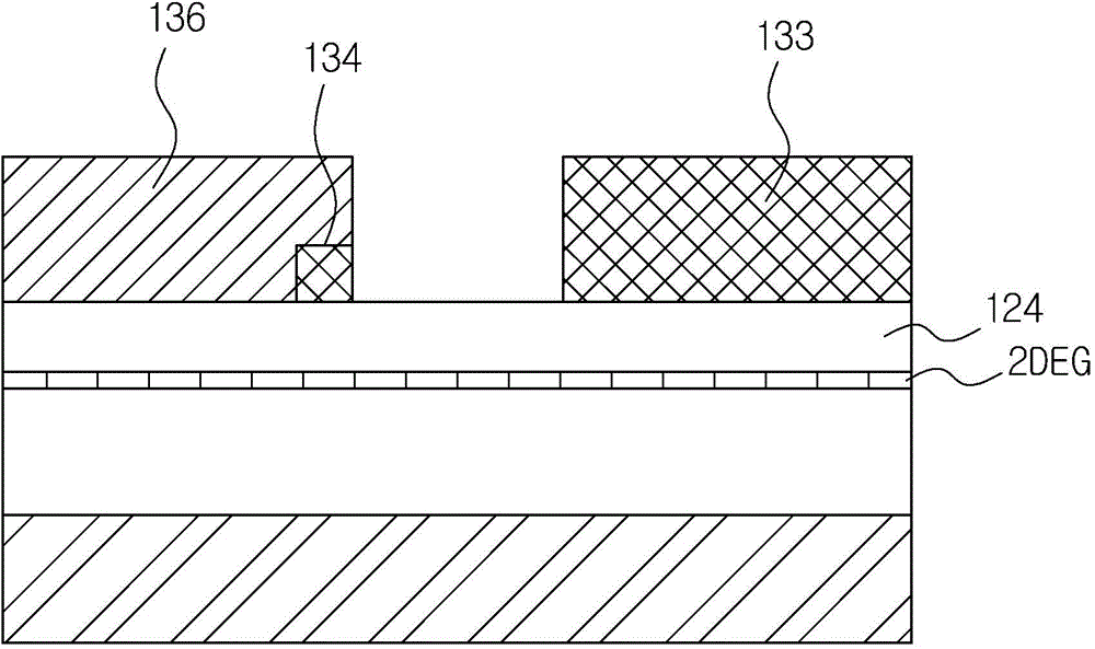
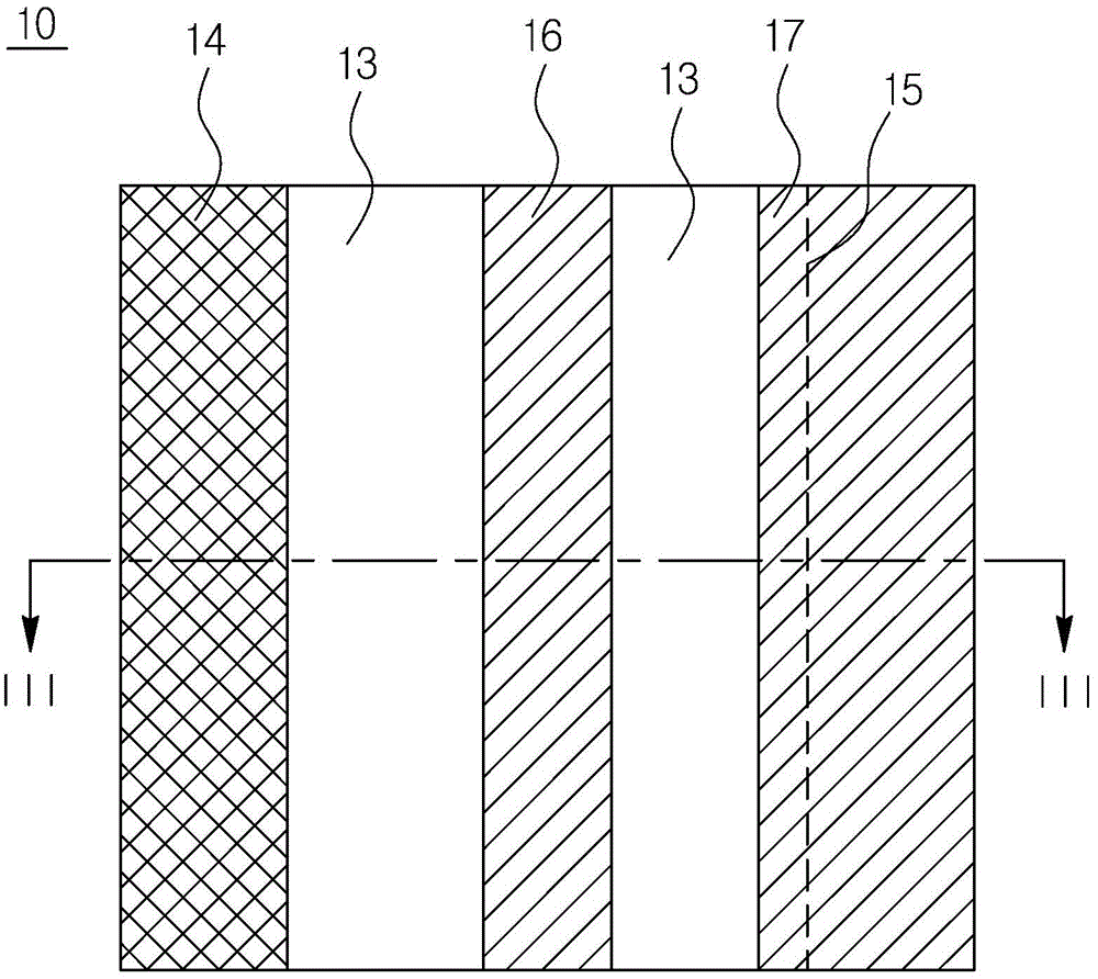
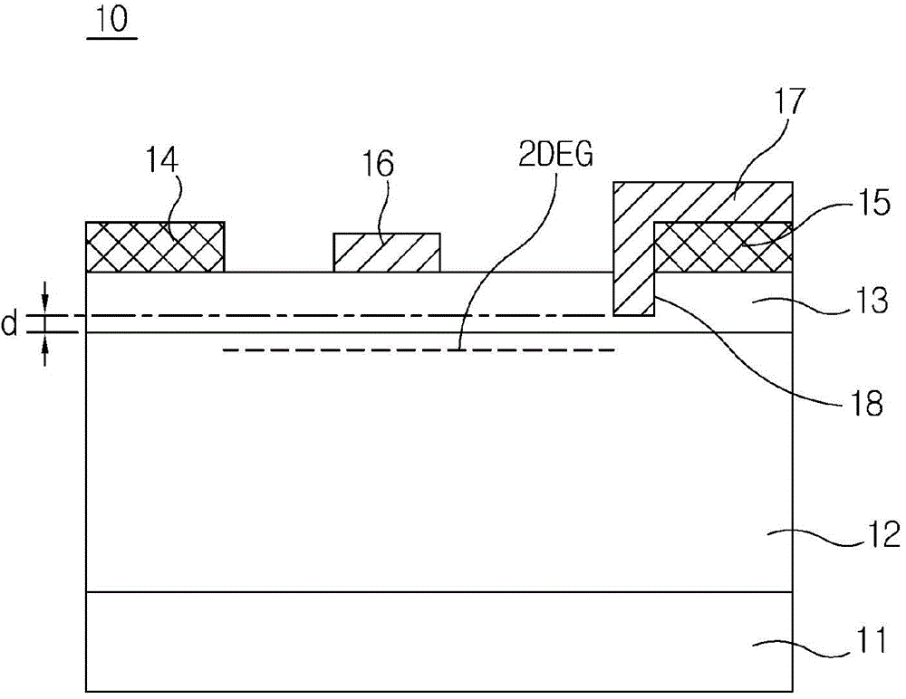
[0092] Hereinafter, preferred embodiments of the present invention will be described in detail with reference to the drawings. For clarity and convenience of description, the width of lines or the size of constituent elements and the like shown in the drawings may be exaggerated.

[0093] The embodiments to be described below are provided as examples in order to fully convey the idea of ​​the present invention to those skilled in the art to which the present invention pertains. Therefore, the present invention is not limited to the Examples described below, and may be embodied in other forms. In addition, in the drawings, for convenience of illustration, the width, length, thickness, etc. of the constituent elements may be expressed exaggeratedly. In addition, when it is stated that one constituent element is located "on" or "on" other constituent elements, it includes not only the case where each part is located "immediately above" or "immediately above" other parts, but als...


PUM


Abstract

Exemplary embodiments of the present invention disclose a unidirectional heterojunction transistor including a channel layer made of a first nitride-based semiconductor having a first energy bandgap, a barrier layer made of a second nitride-based semiconductor having a second energy bandgap different from the first energy bandgap, the barrier layer including a recess, a drain electrode disposed on a first region of the barrier layer, and a recessed-drain Schottky electrode disposed in the recess of the barrier layer, the recessed-drain Schottky electrode contacting the drain electrode.

Description

technical field [0001] The present invention relates to a unidirectional heterojunction transistor, which is a nitride semiconductor device, and a method for manufacturing the same. In particular, it relates to a unidirectional heterojunction transistor capable of preventing reverse leakage current by using a rectifying electrode and a method for manufacturing the same. [0002] Alternatively, the present invention relates to a nitride semiconductor device having a mixed junction drain utilizing a Schottky junction and an Ohmic junction, and a method for manufacturing the same. Background technique [0003] Recently, with the development of information and communication technology, transistors suitable for ultra-high-speed and large-capacity signal transmission and capable of high-speed switching operations and high-voltage transistors suitable for high-voltage environments such as hybrid vehicles are required in various fields. . However, existing silicon-based transistor...

Claims


Application Information

Patent Timeline
Patent Type & Authority Applications(China)
IPC IPC(8): H01L29/778H01L29/47H01L29/423H01L21/335
CPCH01L29/7786H01L29/4236H01L29/66431H01L29/778H01L29/0619H01L29/42316H01L29/1066H01L29/66462H01L29/41766H01L29/2003
Inventor 郭俊植郑暎都车昊映朴奉烈李在吉李宽铉
Owner SEOUL SEMICONDUCTOR
Why Eureka
Try Eureka