Rising edge detection circuit

A one-way, transistor technology, applied in the field of rising edge detection circuit, can solve problems such as unsatisfactory, and achieve the effect of simple structure

Active Publication Date: 2014-09-10
DALIAN UNIV OF TECH
View PDF4 Cites 5 Cited by
  • Summary
  • Abstract
  • Description
  • Claims
  • Application Information

AI Technical Summary

Problems solved by technology

Assuming that the delays of the inverter and the AND gate are both zero, and the delay of the delay unit is the pulse width of the output pulse signal, the pulse width of the output pulse signal must be smaller than the pulse width of the input pulse signal, which cannot meet the requirements of the subsequent equipment for the output pulse signal. The pulse width is greater than the requirement of the pulse width of the input pulse signal

Method used


Image

  • Rising edge detection circuit
  • Rising edge detection circuit
  • Rising edge detection circuit

Examples


Embodiment Construction

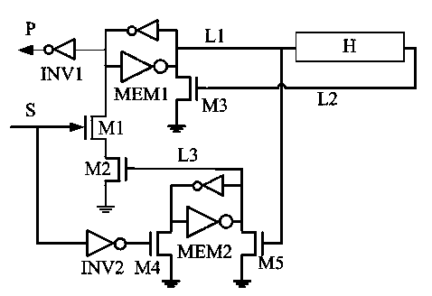
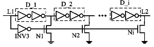
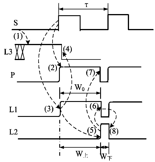
[0010] The specific implementation manner of the present invention will be described below with reference to the accompanying drawings. The basic structure of the present invention is as figure 1 As shown: an input terminal S and an output terminal P are provided, the input terminal S is connected to the gate of the NMOS transistor M1, the source of the NMOS transistor M1 is connected to the drain of the NMOS transistor M2, and the source of the NMOS transistor M2 Grounded, the drain of the NMOS transistor M1 is connected to the bistable memory unit MEM1 one way, and the other is connected to the output terminal P through the inverter INV1; the other end (L1 end) of the bistable memory unit MEM1 is connected to the NMOS transistor The drain of M3 is connected, and the other channel is connected to the gate of NMOS transistor M3 through an asymmetric delay circuit H (the output terminal of asymmetric delay circuit H is L2), and the source of NMOS transistor M3 is grounded; An ...


PUM


Abstract

The invention discloses a rising edge detection circuit which is composed of a bi-stable storage unit, an asymmetric delay unit, an inverter and a plurality of NMOS transistors. As long as an asymmetric delay circuit meets the conditions that the sum of rising edge delay and falling edge delay is larger than the pulse period of input signals and the falling edge delay is very small, output signals with the maximum pulse width close to the pulse period of the input signals can be generated, and the use requirements of a follow-up device can be met. The rising edge detection circuit not only is simple in structure, but also has a self starting function, and the self starting can be achieved when the initial low level length of the input signals is larger than the rising edge delay of the asymmetric delay circuit.

Description

technical field [0001] The invention relates to a rising edge detection circuit, in particular to a rising edge detection circuit whose output signal pulse width is greater than the input signal pulse width. Background technique [0002] The rising edge (or falling edge) detection circuit is a commonly used circuit, which is mainly used to detect whether there is a rising edge pulse in the input signal, and if so, output a pulse signal. The existing rising edge detection circuit consists of a delay unit, an inverter and an AND gate. One path of the input signal is directly connected to the AND gate, and the other path is connected to the AND gate after passing through a delay unit and an inverter in series. Assuming that the delays of the inverter and the AND gate are both zero, and the delay of the delay unit is the pulse width of the output pulse signal, the pulse width of the output pulse signal must be smaller than the pulse width of the input pulse signal, which cannot...

Claims


Application Information

Patent Timeline
Patent Type & Authority Applications(China)
IPC IPC(8): H03K5/1534
CPCH03K5/1534
Inventor 张建伟张修哲吴国强陈晓明苗延楠郑善兴丁秋红潘阿成滕飞李佳琪郑钰芷
Owner DALIAN UNIV OF TECH
Why Eureka
Try Eureka