Organic light-emitting display device

A light-emitting display and organic light-emitting layer technology, which is applied to semiconductor devices, electrical components, circuits, etc., can solve the problems of current magnitude difference, unfavorable light emission of organic light-emitting elements, and inconsistent display brightness of display areas

Active Publication Date: 2014-09-24
WUHAN TIANMA MICRO ELECTRONICS CO LTD +1
View PDF5 Cites 22 Cited by
  • Summary
  • Abstract
  • Description
  • Claims
  • Application Information

AI Technical Summary

Problems solved by technology

The cathodes of multiple organic light-emitting elements are connected together to form a whole-surface cathode layer, and the cathode of each organic light-emitting element is connected to the cathode via hole outside the display area through this entire-surface cathode layer to obtain the cathode from the outside. However, due to the high surface resistance of the transparent conductive material, the cathode driving signal will generate a voltage drop on the cathode layer, and the distance between the cathode of the organic light-emitting element at different positions in the display area and the cathode via hole is different, so it is different. The cathode driving signal of the organic light-emitting element at the position will have different voltage losses on the cathode layer, and the input driving voltage is the same during display, resulting in a difference in the voltage drop on each organic light-emitting element, resulting in a difference in the magnitude of the current, causing The problem of inconsistent display brightness in the display area
Moreover, this inconsistent display brightness will become more obvious as the cathode layer becomes thinner, but the transmittance of an overly thick cathode layer is poor, which is not conducive to the light emission of organic light-emitting elements.

Method used


Image

  • Organic light-emitting display device
  • Organic light-emitting display device
  • Organic light-emitting display device

Examples


Embodiment 1

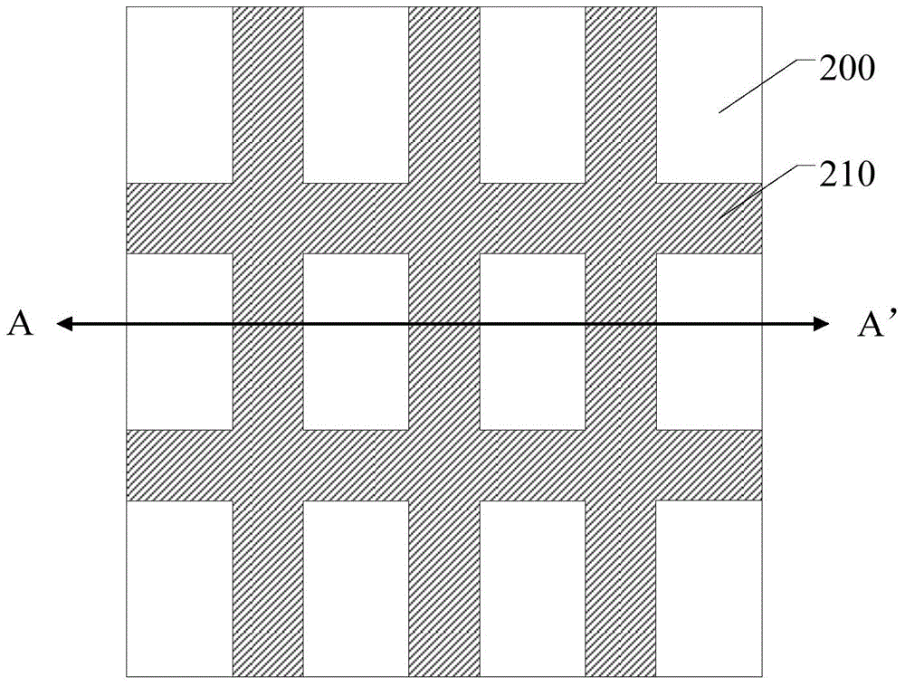
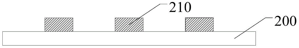
[0021] Please refer to figure 1 , figure 1 It is a schematic top view of the cover plate of the organic light-emitting display device provided in Embodiment 1 of the present invention, figure 2 for figure 1 A cross-sectional view of the cover plate in AA' direction, the cover plate includes a second substrate 200 and a conductive layer 210, and the conductive layer 210 is disposed on the side of the second substrate 200 facing the first substrate.

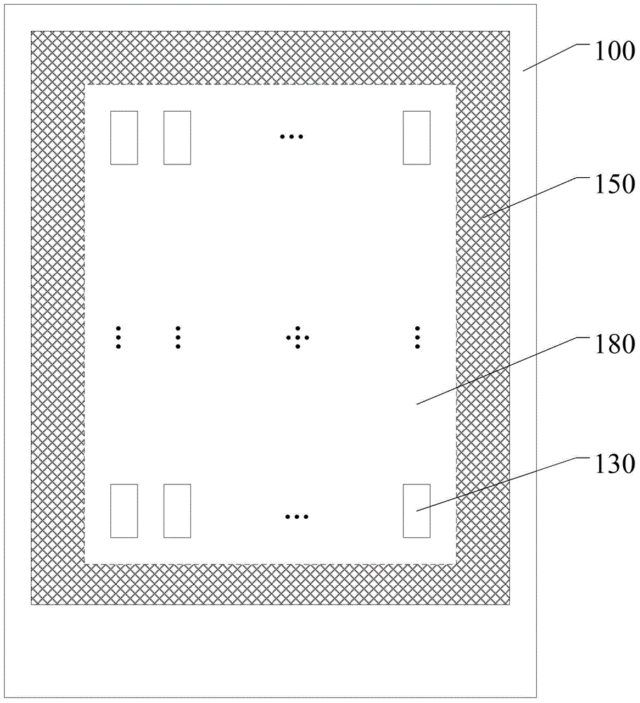
[0022] image 3 It is a top view schematic diagram of an array substrate of an organic light emitting display device provided in Embodiment 1 of the present invention. The array substrate and the cover plate are arranged opposite to each other. The array substrate includes a first substrate 100, a plurality of organic light emitting elements 130 and cathode via holes 150. The plurality of organic light emitting elements 130 and cathode vias 150 are disposed on the side of the first substrate 100 facing the second substrate 200 ...

Embodiment 2

[0030] refer to Figure 7 and Figure 8 , Figure 7 It is a top view schematic diagram of the cover plate of the organic light emitting display device provided in the second embodiment, Figure 8 for Figure 7 Sectional view of the middle cover along the direction of BB'. The organic light-emitting display device provided in the second embodiment is based on the first embodiment, and the thickness of the conductive layer 310 corresponding to different positions of the display area is different, and the variation trend of the thickness is related to the position of the cathode via hole.

[0031] Figure 7 and Figure 8 shows the case where the cathode vias are around the display area, Figure 7 Among them, the area shown in area 350 is the area corresponding to the cathode via hole. Specifically, when the array substrate and the cover plate are arranged oppositely, the area 350 corresponding to the cathode via hole corresponds to the area of ​​the cathode via hole in the ...

Embodiment 3

[0038] refer to Figure 9 , Figure 9 It is a schematic plan view of a cover plate of an organic light emitting display device provided in Embodiment 3 of the present invention. The thickness of the conductive layer 410 of the organic light-emitting display device provided in Embodiment 3 is the same, but the arrangement density of the conductive layer 410 at different positions in the display area is changed, and the distribution density of the conductive layer 410 on the cover plate in the display area is not uniform, and the change trend is It is related to the position of the cathode via.

[0039] Figure 9 shows the case where the cathode vias are around the display area, Figure 9 Among them, the area 450 is the area corresponding to the cathode via hole. Specifically, when the array substrate and the cover plate are arranged oppositely, the area 450 corresponding to the cathode via hole corresponds to the cathode via hole area of ​​the array substrate, and is the pro...


PUM


Abstract

The invention provides an organic light-emitting display device. The organic light-emitting display device comprises a first substrate, a second substrate, a plurality of organic light-emitting elements and a conductive layer. The first substrate and the second substrate are arranged oppositely. The organic light-emitting elements are arranged on the side, facing the second substrate, of the first substrate. Each organic light-emitting element comprises an anode arranged on the first substrate, an organic light-emitting layer arranged on the anode and a cathode arranged on the organic light-emitting layer. The conductive layer is arranged on the side, facing the first substrate, of the second substrate. The conductive layer makes contact with the cathodes. Due to the fact that the conductive layer makes contact with the cathodes, sheet resistance of cathode layers can be reduced, and voltage drop, on the cathode layers, of driving signals can be reduced. Thus, the difference of values of currents flowing through all the organic light-emitting elements is reduced, light emitted by the organic light-emitting elements are more similar in intensity, and the display brightness of the whole organic light-emitting device tends to be uniform.

Description

technical field [0001] The present invention relates to the field of organic light-emitting display, and more specifically, relates to an organic light-emitting display device displaying a more uniform top emission structure. Background technique [0002] Organic Light Emitting Display (OLED, Organic Light Emitting Display) is a thin-film light-emitting device made of organic semiconductor material and driven by DC voltage, which has the characteristic of self-luminescence. [0003] An organic light-emitting display device with self-luminous properties includes an organic light-emitting element including an organic light-emitting layer, an anode, and a cathode. Organic light-emitting display devices are classified into top-emission structures and bottom-emission structures according to different light emitting directions of organic light-emitting elements. The light emitted by the organic light-emitting element in the top-emission organic light-emitting display device is em...

Claims


Application Information

Patent Timeline
Patent Type & Authority Applications(China)
IPC IPC(8): H01L51/52H01L27/32
CPCH10K50/82
Inventor 熊志勇钱栋
Owner WUHAN TIANMA MICRO ELECTRONICS CO LTD
Why Eureka
Try Eureka