

Parallel test system and testing method thereof
A test system and wafer carrying technology, applied in the direction of semiconductor/solid-state device testing/measurement, single semiconductor device testing, etc., can solve problems such as body contact with moving knobs, wafer carrier plate movement, probe card damage, etc. achieve the effect of avoiding damage
- Summary
- Abstract
- Description
- Claims
- Application Information
AI Technical Summary
Problems solved by technology
Method used
Image

Examples
Embodiment Construction
[0019] In order to illustrate the technical content, structural features, achieved goals and effects of the present invention in detail, the following will be described in detail in conjunction with the embodiments and accompanying drawings.
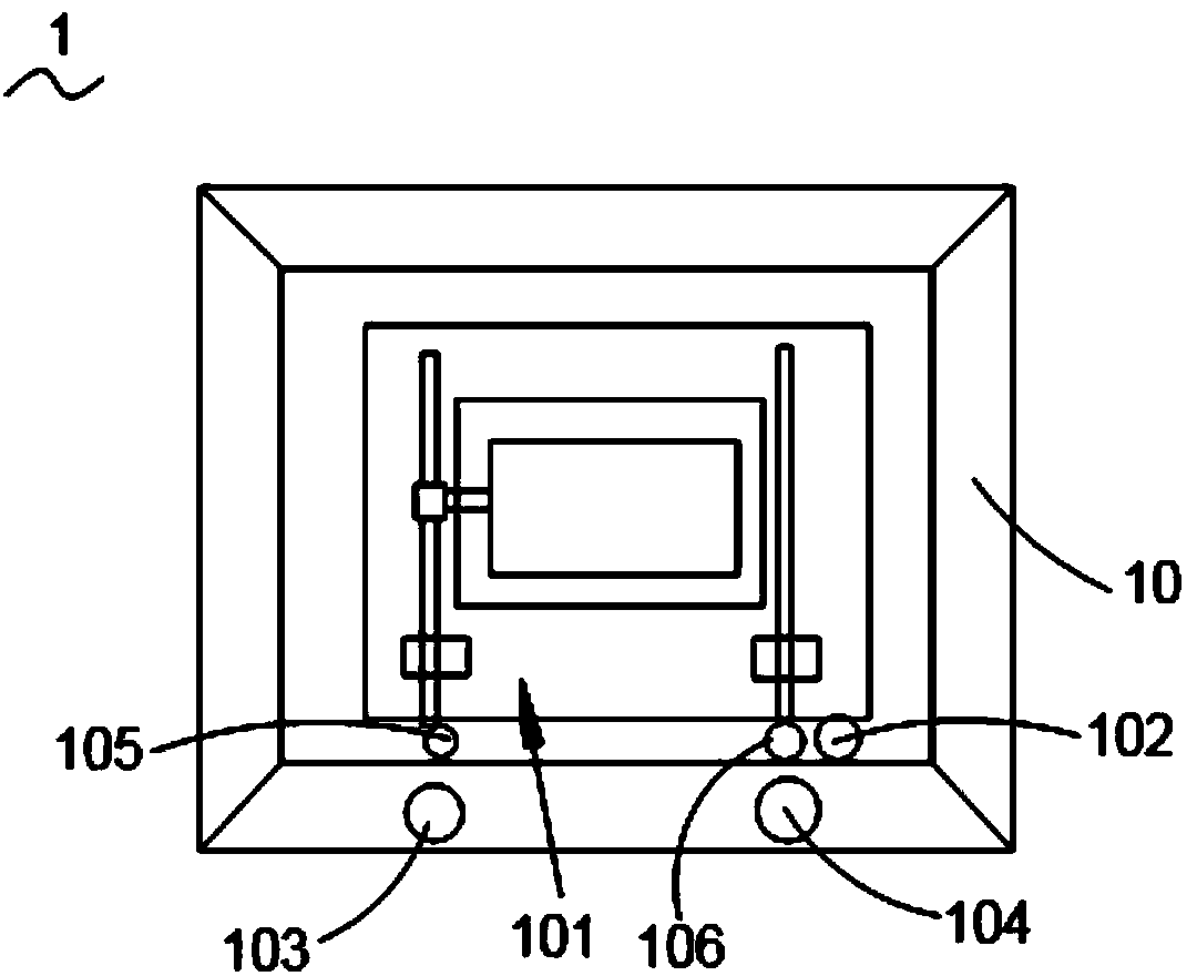
[0020] see Figure 1 ~ Figure 3 , figure 1 Shown is a schematic structural diagram of the parallel testing system of the present invention. Figure 2(a) ~ Figure 2(b) Shown is a schematic structural diagram of the locking component of the parallel testing system of the present invention. image 3 Shown is a cross-sectional view of the parallel testing system of the present invention. The parallel test system 1 includes: a housing 10, the housing 10 encloses and forms an accommodating space 101, and the wafer carrying platform lifting knob 102 is arranged at intervals on the housing 10, and the wafer carrying platform moves left and right Knob 103, knob 104 for moving the wafer carrying platform back and forth; wafer carrying tray 11,...
PUM
 Abstract
Description
Claims
Application Information