

A semiconductor material baf x znas and preparation method thereof
A semiconductor and crystal structure technology, applied in polycrystalline material growth, chemical instruments and methods, self-solid, etc., can solve the problems of difficult stable existence, poor stability, difficult high purity of semiconductor materials, etc., and achieve good stability
- Summary
- Abstract
- Description
- Claims
- Application Information
AI Technical Summary
Problems solved by technology
Method used
Image

Examples
Embodiment 1
[0041] This embodiment provides a method for preparing a semiconductor material, including:
[0042] 1) Dissolve 1.753 g of BaF in an argon-filled glove box 2 Powder, 4.119 grams of Ba block, 2.616 grams of Zn powder, and 2.996 grams of As powder were uniformly mixed, and the mixture was pressed into an alumina ceramic test tube;
[0043] 2) Vacuum seal the ceramic test tube with the sample in the quartz tube, fill the quartz tube with argon and seal it;
[0044] 3) Sinter the quartz tube in a high temperature furnace at 600°C for 20 hours. After the sintering is completed, the semiconductor material BaF is obtained. 0.5 ZnAs.
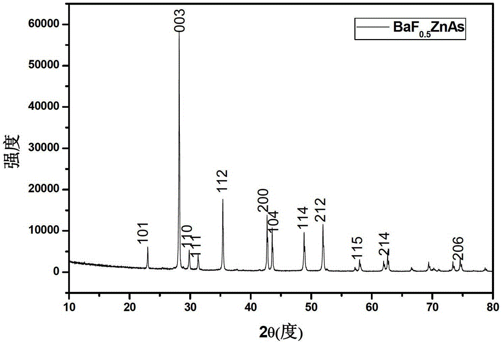
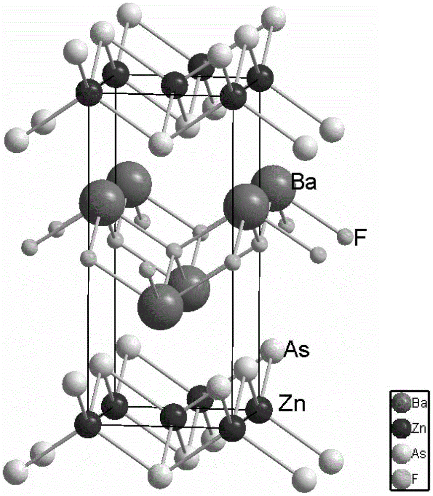
[0045] The X-ray diffraction pattern of the sample is as figure 1 shown, from figure 1 It can be seen that all the diffraction peaks of this sample can find the corresponding diffraction index, and there is no impurity, indicating that the method provided in this example has prepared a high-purity semiconductor material BaF 0.5 ZnAs, crystal struc...
Embodiment 2
[0048] This embodiment provides a method for preparing a semiconductor material, including:
[0049] 1) Dissolve 2.6295 g of BaF in an argon-filled glove box 2 powder, 0.6865 g of Ba block, 1.308 g of Zn powder, and 1.498 g of As powder were evenly mixed, and the mixture was put into an alumina ceramic test tube;
[0050] 2) Vacuum seal the ceramic test tube with the sample in the quartz tube, fill the quartz tube with argon and seal it;
[0051] 3) Sinter the quartz tube in a high temperature furnace at 1000°C for 5 hours. After the sintering is completed, the semiconductor material BaF is obtained. 1.5 ZnAs.
[0052] The X-ray diffraction pattern of the sample is as Figure 5 shown, from Figure 5 It can be seen that all the diffraction peaks of this sample can find the corresponding diffraction index, and there is no impurity phase, indicating that the method provided in this example has prepared a high-purity semiconductor material BaF 1.5 ZnAs, crystal structure as f...
Embodiment 3
[0054] This embodiment provides a method for preparing a semiconductor material, including:
[0055] 1) Dissolve 2.804 g of BaF in an argon-filled glove box 2 Powder, 3.2952 grams of Ba block, 2.616 grams of Zn powder, and 2.996 grams of As powder are evenly mixed, and the mixture is packed into a niobium tube, and the niobium tube is sealed under the protection of an inert gas;
[0056] 2) Vacuum seal the niobium tube with the sample in the quartz tube, fill the quartz tube with argon and seal it;
[0057] 3) Sinter the quartz tube at a temperature of 900°C in a high-temperature furnace for 20 hours;
[0058] 4) After the sintering is completed, the obtained sample is ground, mixed and pressed into tablets under the protection of argon gas, and put into a niobium tube, and the niobium tube is sealed under the protection of argon gas;
[0059] 5) Vacuum seal the niobium tube with the sample in the quartz tube, fill the quartz tube with argon and seal it;
[0060] 6) Sinter ...
PUM
 Abstract
Description
Claims
Application Information