Supercharge Your Innovation With Domain-Expert AI Agents!

Manufacture method of planar optical waveguide

A planar optical waveguide and manufacturing method technology, applied in the direction of light guides, optics, optical components, etc., can solve the problems of high manufacturing cost of planar optical waveguides, prevent over-etching or under-etching, reduce production costs, and reduce usage Effect

Active Publication Date: 2014-10-15
SOLOREIN TECH
View PDF4 Cites 7 Cited by
  • Summary
  • Abstract
  • Description
  • Claims
  • Application Information

AI Technical Summary

Problems solved by technology

However, the use of a large amount of etching reagents leads to higher production costs of planar optical waveguides.

Method used


Image

  • Manufacture method of planar optical waveguide
  • Manufacture method of planar optical waveguide
  • Manufacture method of planar optical waveguide

Examples


Embodiment Construction

[0029] The following will clearly and completely describe the technical solutions in the embodiments of the present invention with reference to the accompanying drawings in the embodiments of the present invention. Obviously, the described embodiments are only some, not all, embodiments of the present invention. Based on the embodiments of the present invention, all other embodiments obtained by persons of ordinary skill in the art without making creative efforts belong to the protection scope of the present invention.

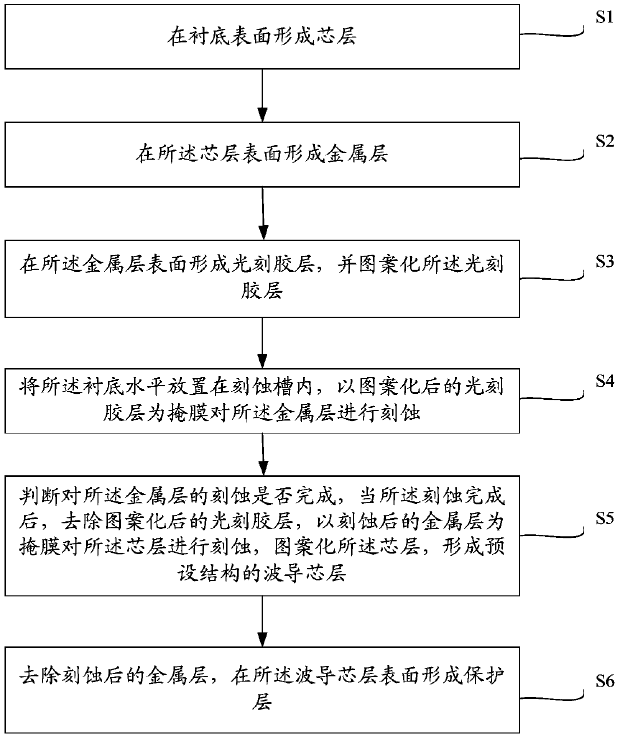
[0030] An embodiment of the present application provides a method for manufacturing a planar optical waveguide, the method comprising:

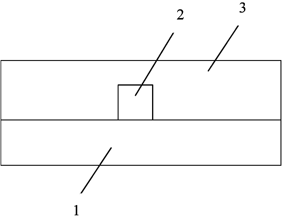
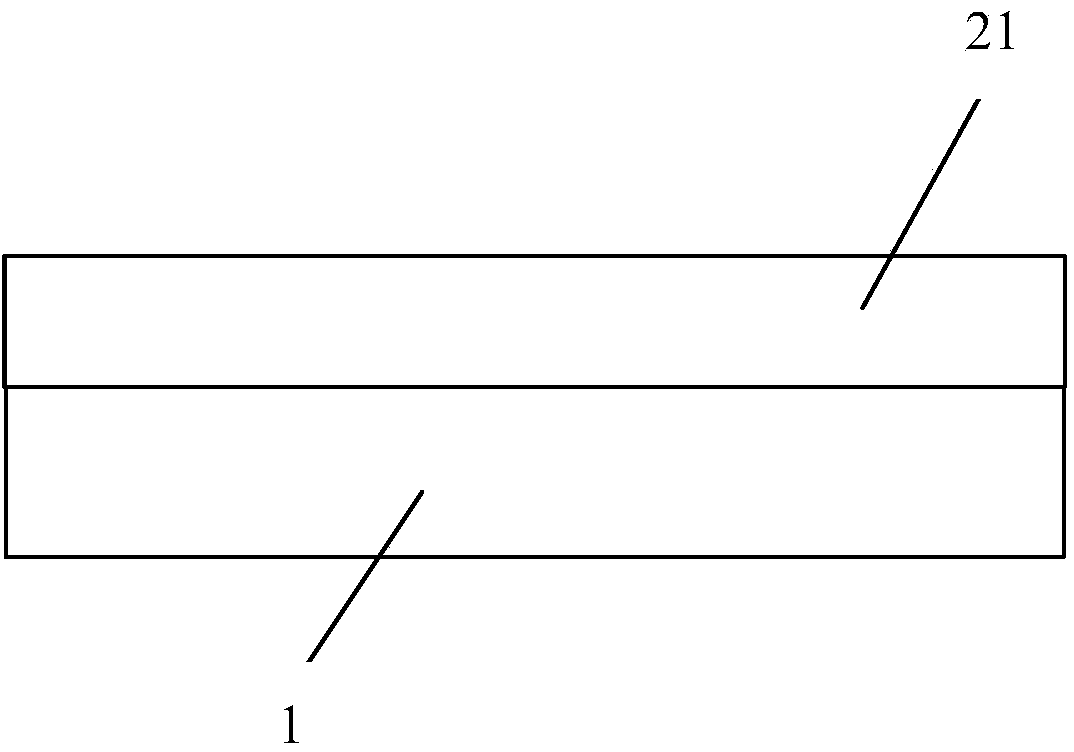
[0031] Step S1: Reference figure 2 , forming a core layer 21 on the surface of the substrate 1 .

[0032] The core layer 21 can be formed on the surface of the substrate by PECVD process. The core layer 21 is used to prepare a waveguide core layer of a planar optical waveguide, and the core layer 21 is a doped silicon diox...


PUM


Abstract

The invention discloses a manufacture method of a planar optical waveguide. The manufacture method of the planar optical waveguide includes: forming a core layer on the surface of a substrate; forming a metal layer on the surface of the core layer; forming an optical resist layer on the surface of the metal layer, and patterning the optical resist layer; horizontally placing the substrate in an etching groove, and etching the metal layer by using the patterned optical resist layer as a photo mask; judging whether etching on the metal layer is completed, removing the patterned optical resist layer after the etching is completed, using the etched metal layer as a photo mask to etch the core layer, and patterning the core layer so as to form a waveguide core layer of preset structure; removing the etched metal layer and forming a protection layer on the surface of the waveguide core layer, wherein the surface of the substrate, provided with the metal layer, is placed upwards, and the metal layer is immersed into a metal etching reagent in the etching groove. The manufacture method of the planar optical waveguide reduces manufacture cost of the planar optical waveguide.

Description

technical field [0001] The invention relates to the technical field of semiconductor device manufacturing technology, and more specifically, relates to a method for manufacturing a planar optical waveguide. Background technique [0002] Planar optical waveguide devices are widely used in optical modulators, optical switches, optical power splitters, optical couplers, wavelength division multiplexers, optical filters, polarization divisions, etc. due to their small size, high integration, and good reliability. Optical products such as beamers and microlenses. refer to figure 1 , figure 1 It is a schematic structural diagram of a planar optical waveguide, including: a substrate 1 ; a waveguide core layer 2 arranged on the surface of the substrate 1 ; and a protective layer 3 covering the surface of the waveguide core layer 2 . [0003] When preparing an optical waveguide device, it is necessary to prepare a metal mask layer so as to form a waveguide core layer with a predet...

Claims


Application Information

Patent Timeline
Patent Type & Authority Applications(China)
IPC IPC(8): G02B6/136
Inventor 冯春蓉向舟翊李朝阳
Owner SOLOREIN TECH
Features
  • R&D
  • Intellectual Property
  • Life Sciences
  • Materials
  • Tech Scout
  • Unparalleled Data Quality
  • Higher Quality Content
  • 60% Fewer Hallucinations
Learn More