Electric fuse structure and method of forming the same

An electric fuse and fork-shaped technology, applied in the field of electric fuse structure and its formation, can solve the problems of complex fusing process, destructive laser cutting, unfavorable chip miniaturization, etc., and achieve the goal of controlling uniformity and improving stability Effect

Active Publication Date: 2016-12-28
SEMICON MFG INT (SHANGHAI) CORP
View PDF5 Cites 0 Cited by
  • Summary
  • Abstract
  • Description
  • Claims
  • Application Information

AI Technical Summary

Problems solved by technology

Due to the high destructiveness of laser cutting, in order to ensure that other devices in the chip are not indirectly damaged during cutting, there must be a large enough space between the cut metal fuse and other devices, and the chip needs to be repaired after cutting. The fusing process is more complicated, which is not conducive to the miniaturization of the chip
For polysilicon fuses, as the size of MOS devices continues to decrease, the CMOS process gradually transitions from polysilicon gate technology to metal gate technology. The formation of polysilicon fuses in integrated circuits is not compatible with metal gate technology, requiring additional process steps and process costs

Method used


Image

  • Electric fuse structure and method of forming the same
  • Electric fuse structure and method of forming the same
  • Electric fuse structure and method of forming the same

Examples


Embodiment Construction

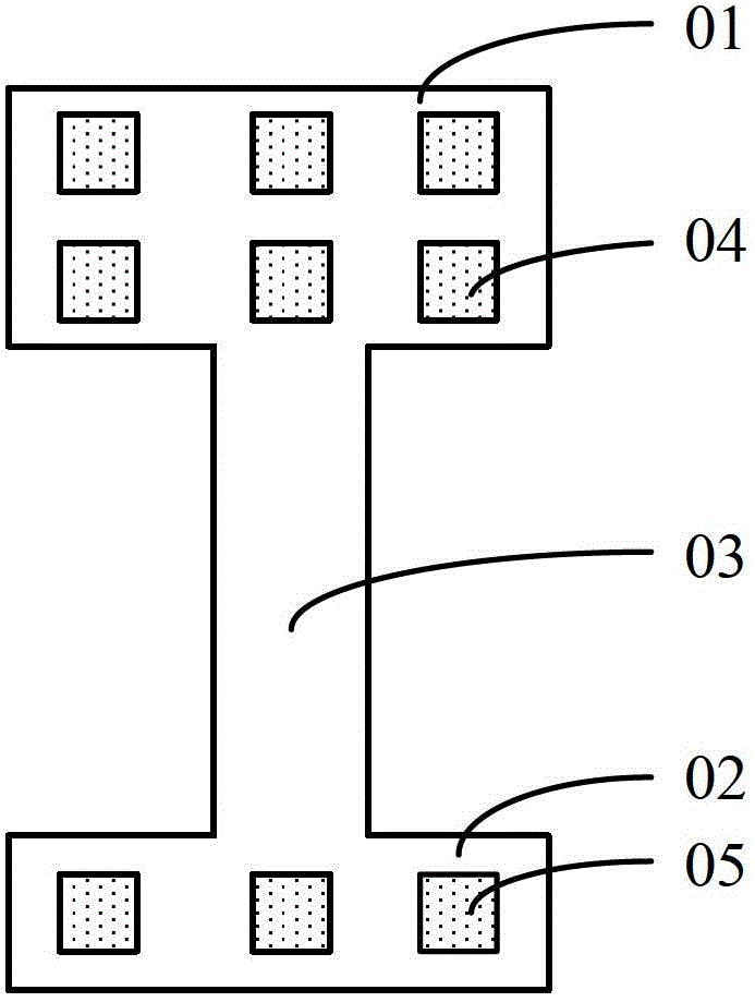
[0033] Since the formation process of the polysilicon fuse is not compatible with the existing metal gate process, and the metal fuse is not conducive to the miniaturization of the chip, and the chip needs to be repaired after laser cutting, the fusing process is more complicated. Therefore, the inventor has studied , an electric fuse structure is proposed, comprising: a substrate, a first conductive layer located on the surface of the substrate, the first conductive layer has an anode, a cathode and an interconnection structure connecting the anode and the cathode; The first conductive plug on the surface of the cathode and the second conductive plug on the surface of the anode, the number of the first conductive plug is 1, and the number of the second conductive plug is greater than 1, so that the first The current density flowing through the conductive plug is far greater than the current density flowing through the second conductive plug, and the contact between the first c...


PUM


Abstract

An electric fuse structure and its forming method, the electric fuse structure comprising: a substrate, a first conductive layer located on the surface of the substrate, an interlayer dielectric layer covering the first conductive layer and the substrate, located on the The first conductive plug on the surface of the first conductive layer and through the interlayer dielectric layer, the second conductive layer located on the surface of the first conductive plug and the interlayer dielectric layer, wherein the first conductive layer and the first conductive A bottom surface portion of the plug is in contact or the second conductive layer is in contact with a top surface portion of the first conductive plug. Since the first conductive plug is in partial contact with the first conductive layer and the second conductive layer, the positional resistance of the partial contact is greater, the electric field strength is greater, and the rate of electromigration is faster, so that the position of the partial contact It is easier to be fused, the fusing time is shortened, and it is easier to control.

Description

technical field [0001] The invention relates to the field of semiconductors, in particular to an electric fuse structure and a forming method thereof. Background technique [0002] With the continuous reduction of feature size, semiconductor devices are more and more susceptible to the influence of impurities or defects in the silicon substrate, and the failure of a single diode, MOS transistor, or memory cell often leads to the failure of the entire integrated circuit chip. In order to solve the above problems and improve the yield, some redundant circuits are often formed in the integrated circuit chip. When the manufacturing process is completed and it is found that some devices cannot work normally, the fuse can be used to electrically isolate the failed circuit from other circuit modules, and the redundant circuit can be used to replace the original failed circuit. Especially in the manufacturing process of memory, due to the large number of memory cells, it is inevita...

Claims


Application Information

Patent Timeline
Patent Type & Authority Patents(China)
IPC IPC(8): H01L23/525H01L21/768
Inventor 甘正浩徐依协朱志炜
Owner SEMICON MFG INT (SHANGHAI) CORP
Why Eureka
Try Eureka