Substrate carrying device and substrate carrying method utilizing the same

A technology for substrate handling and substrate support, which is applied in the directions of transportation and packaging, program control manipulators, lighting and heating equipment, etc., can solve the problems of increasing the time for handling substrates 100, reducing the productivity and qualification rate of electronic components, and improving productivity and qualification. efficiency, increase speed, and reduce process costs

Inactive Publication Date: 2014-10-22
HYUNDAI HEAVY IND CO LTD
View PDF10 Cites 0 Cited by
  • Summary
  • Abstract
  • Description
  • Claims
  • Application Information

AI Technical Summary

Problems solved by technology

However, according to this solution, the substrate transfer device 10 related to the prior art increases the time required to transfer the substrate 100, resulting in reduced productivity and yield of the electronic components.

Method used


Image

  • Substrate carrying device and substrate carrying method utilizing the same
  • Substrate carrying device and substrate carrying method utilizing the same
  • Substrate carrying device and substrate carrying method utilizing the same

Examples


Embodiment Construction

[0044] Embodiments of the substrate transfer device according to the present invention will be described in detail below with reference to the drawings.

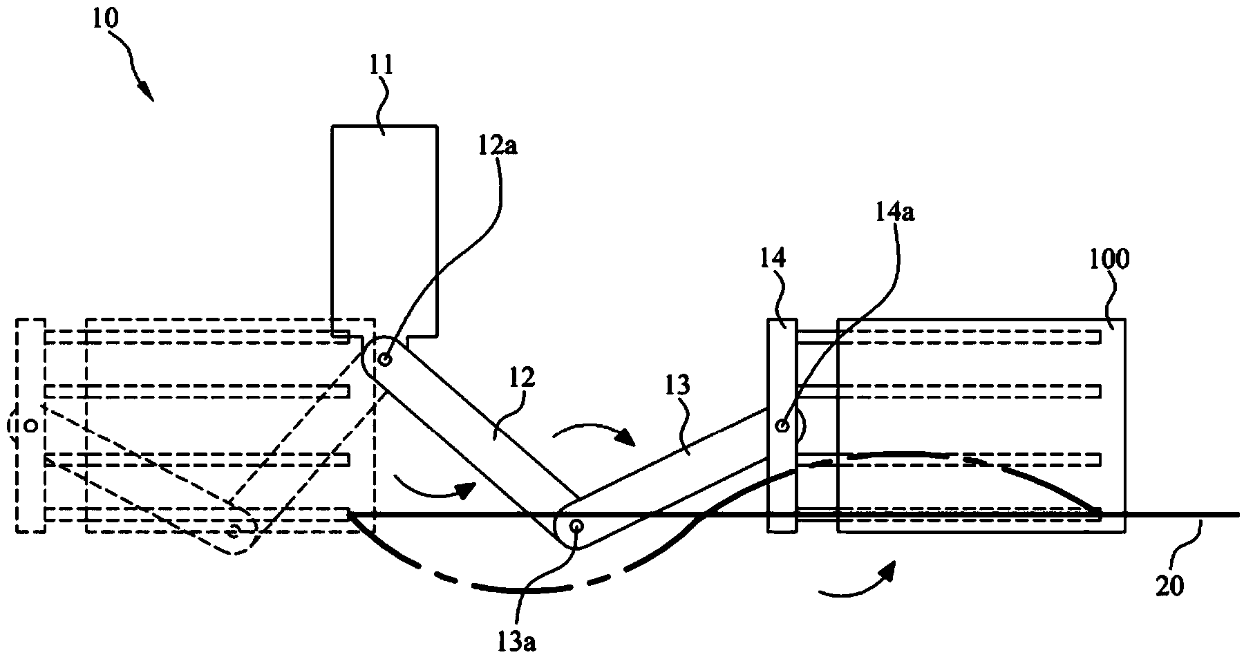
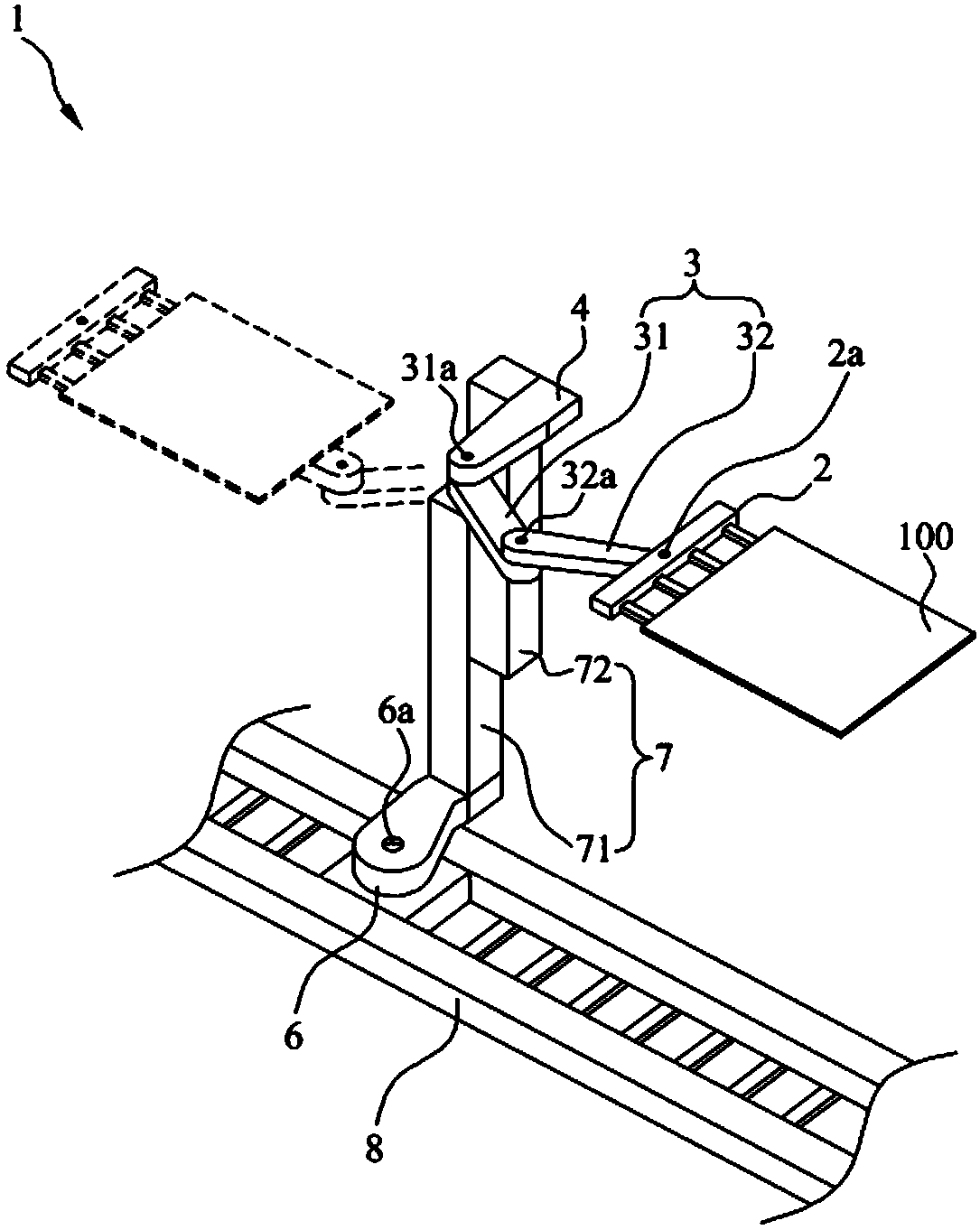
[0045] refer to Figure 2 to Figure 5 , the substrate transfer device 1 according to the present invention is used to transfer a substrate 100 . The substrate 100 is used to manufacture electronic components such as display devices, solar cells, and semiconductor elements. For example, the substrate transfer device 1 according to the present invention can transfer the substrate 100 between chambers in which manufacturing processes such as a deposition device and an etching device are performed on the substrate 100 .

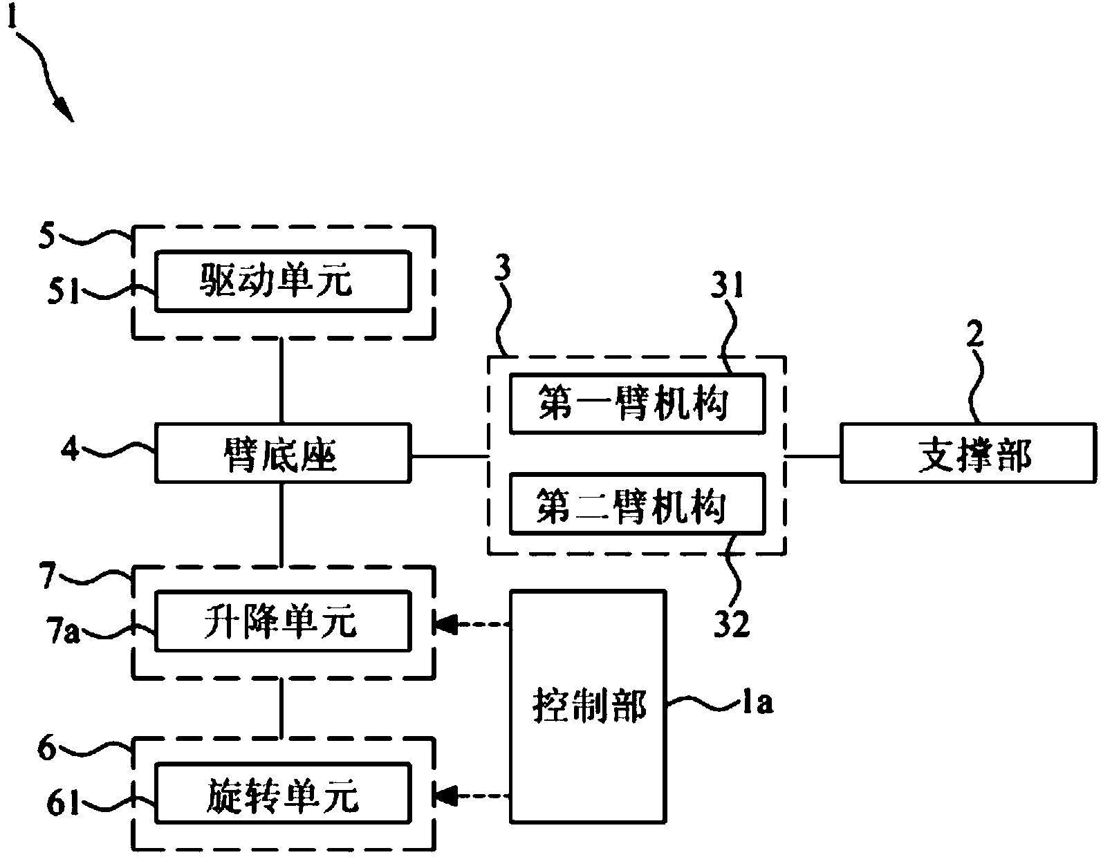
[0046] The substrate transfer device 1 according to the present invention includes: a support part 2 for supporting the substrate 100; an arm unit 3 for rotatably combining the support part 2; an arm base 4 for rotatably connecting the arm unit 3 Combination; drive part 5, in order to move the support part 2,...


PUM


Abstract

The invention relates to a substrate carrying device and a substrate carrying method utilizing the same. The substrate carrying device comprises a supporting portion for supporting substrates; an arm unit, wherein the supporting portion can be combined with the arm unit in a rotatable manner; an arm pedestal, wherein the arm unit can be combined with the arm pedestal in a rotatable manner; and a driving portion which enables the arm unit and the supporting portion to rotate so as to move the supporting portion. While the driving portion is moving the supporting portion, the supporting portion is moved in a direction opposite to a snaking direction of the supporting portion.

Description

technical field [0001] The present invention relates to a substrate conveying device and a substrate conveying method for conveying a substrate in a manufacturing process of an electronic component. Background technique [0002] Display devices, solar cells, semiconductor elements, etc. (hereinafter referred to as "electronic components") are manufactured through various processes. A substrate for manufacturing the electronic component is used in such a process. For example, the manufacturing process may include a deposition process of depositing thin films such as conductors, semiconductors, and dielectrics on a substrate, an etching process of forming predetermined patterns with the deposited thin films, and the like. This manufacturing process is done in the process chamber where the related process is carried out. A substrate transfer device is used to transfer substrates between the chambers. [0003] figure 1 It is a plan view of the board|substrate conveyance appa...

Claims


Application Information

Patent Timeline
Patent Type & Authority Applications(China)
IPC IPC(8): B65G49/05
CPCB25J9/042B25J9/106B25J9/1633B25J11/0095H01L21/67742H01L21/68707
Inventor 金兑炫金东赫金祥铉
Owner HYUNDAI HEAVY IND CO LTD
Why Eureka
Try Eureka