
Low-color-error liquid crystal array substrate and drive method thereof

A technology of liquid crystal array and driving method, which is applied in the directions of optics, instruments, electrical components, etc., can solve the problems of rising cost, affecting the pixel aperture ratio, and increasing the probability of occurrence, so as to save costs, reduce the incidence of GDS defects, and reduce color shift Effect

Active Publication Date: 2014-10-29
SHENZHEN CHINA STAR OPTOELECTRONICS TECH CO LTD
View PDF5 Cites 13 Cited by
  • Summary
  • Abstract
  • Description
  • Claims
  • Application Information

AI Technical Summary

Problems solved by technology

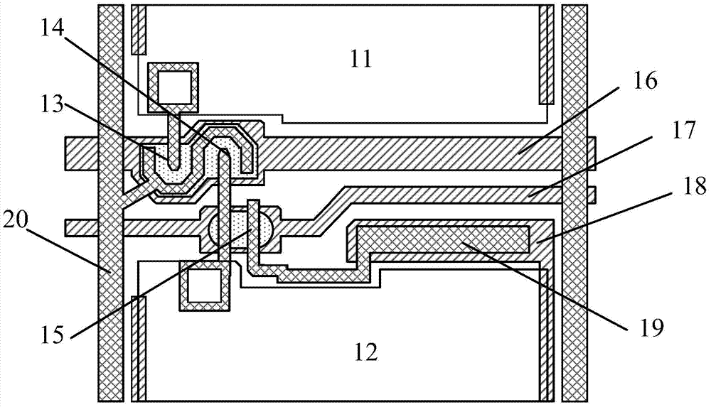
[0005] The disadvantage of the above design is that the sub-gate line 17 will increase the overlapping area with the data line 20, which not only affects the aperture ratio of the pixel, but also causes the probability of a short circuit (Gate-Drain Short, GDS) between the gate line and the data line 20. increase, the cost of associated product manufacturing has risen sharply

Method used


Image

  • Low-color-error liquid crystal array substrate and drive method thereof
  • Low-color-error liquid crystal array substrate and drive method thereof
  • Low-color-error liquid crystal array substrate and drive method thereof

Examples


Embodiment Construction

[0024] The following descriptions of the various embodiments refer to the accompanying drawings to illustrate specific embodiments in which the present invention can be practiced. The directional terms mentioned in the present invention, such as "up", "down", "front", "back", "left", "right", "inside", "outside", "side", etc., are for reference only The orientation of the attached schema. Therefore, the directional terms used are used to illustrate and understand the present invention, but not to limit the present invention. In the figures, structurally similar units are denoted by the same reference numerals.

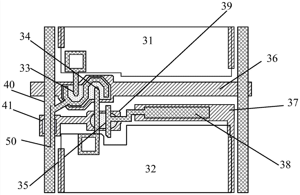
[0025] The liquid crystal array substrate of the present invention includes a plurality of pixel structures, figure 2 A schematic diagram of each pixel structure is shown, each pixel structure includes a main pixel area 31 and a sub-pixel area 32, a gate line 36 is arranged between the main pixel area 31 and the sub-pixel area 32, and the gate line 36 respectively ...


PUM


Abstract

The invention relates to a low-color-error liquid crystal array substrate and a corresponding drive method. The low-color-error liquid crystal array substrate comprises a plurality of pixel structures, each pixel structure comprises a primary pixel area and a secondary pixel area, a gate line is arranged between each primary pixel area and the corresponding secondary pixel area and is provided with a first thin film transistor and a second thin film transistor which are connected to the primary pixel area and the secondary pixel area respectively, the position between each gate line and the corresponding secondary pixel area further comprises a public electrode wire and a metal component, each public electrode wire is provided with a standoff capacitor, and each metal component is provided with a share thin film transistor connected with the corresponding standoff capacitor and electrically connected with a data line through a through hole. Through the design of omitting a sub gate line, switches of the share thin film transistors are switched on directly through signal voltage of the data lines; the inconformity of voltage between each primary pixel area and the corresponding secondary pixel area is solved by adjusting the gate source capacitance of the thin film transistor in the primary pixel area, the aperture opening ratio is improved, and the processing cost is lowered.

Description

technical field [0001] The invention relates to a low color shift liquid crystal array substrate and a corresponding driving method thereof, in particular to a pixel structure in which sub-gate lines are omitted. Background technique [0002] With the development of the information society, people's demand for display equipment is increasing year by year, which promotes the rapid development of LCD panels, and the size of the panels is getting bigger and bigger, especially the requirements for wide viewing angles and low energy consumption are getting higher and higher. Therefore, the design of the pixel structure of the thin film transistor (TFT) device and the liquid crystal panel is also developing towards diversification. [0003] A general liquid crystal electronic device has a display mode with a wide viewing angle. In the display mode with a wide viewing angle, the liquid crystal molecules observed at different viewing angles have different orientations, resulting in ...

Claims


Application Information

Patent Timeline
IPC IPC(8): G02F1/1362G02F1/1368G02F1/133H01L27/12
CPCG02F1/1362G02F1/1368
Inventor 柴立
Owner SHENZHEN CHINA STAR OPTOELECTRONICS TECH CO LTD
Learn More