

Semiconductor memory device
A storage device and semiconductor technology, applied in information storage, static memory, digital memory information, etc., can solve problems such as increased power consumption, and achieve the effect of preventing malfunction
- Summary
- Abstract
- Description
- Claims
- Application Information
AI Technical Summary
Problems solved by technology
Method used
Image

Examples
no. 1 Embodiment approach
[0031]
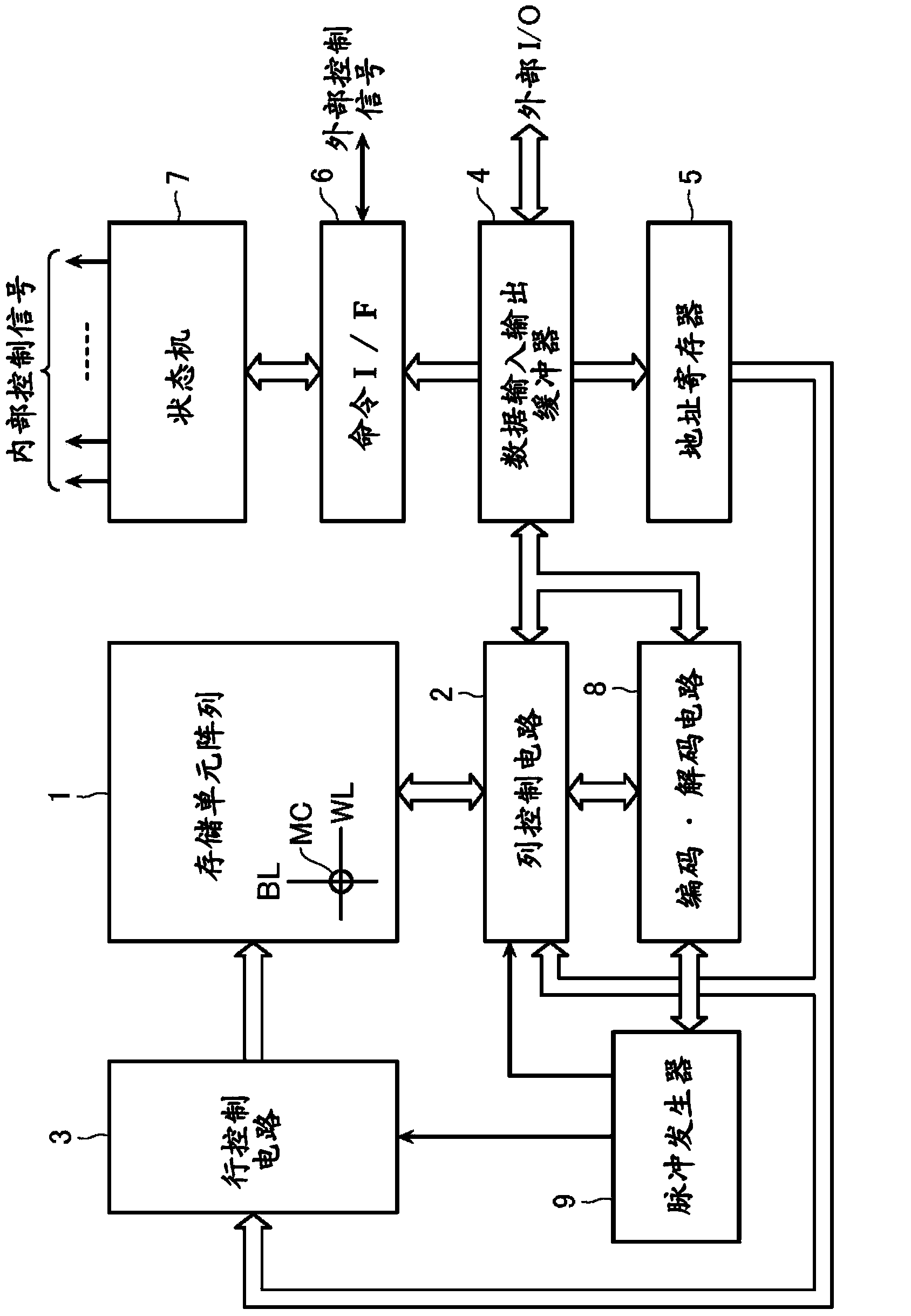
[0032] figure 1 It is an example of a block diagram of the nonvolatile semiconductor memory device according to the first embodiment.
[0033] This nonvolatile semiconductor memory device includes a memory cell array 1 including a plurality of word lines WL, a plurality of bit lines BL intersecting the word lines WL, and a plurality of memory cell arrays provided on the word lines WL and bit lines BL. A plurality of memory cells MC at the intersection.
[0034] In the position adjacent to the bit line BL of the memory cell array 1, there is provided a memory cell that controls the bit line BL of the memory cell array 1 and performs data erasing, data writing, and self-storage of the memory cell MC. Column control circuit 2 for data readout of cell MC.
[0035] In addition, in the position adjacent to the word line WL direction of the memory cell array 1, there are provided the word line WL of the memory cell array 1 and the data erasing of the memory cell MC, the ...
no. 2 Embodiment approach
[0088] Next, referring to the semiconductor memory device according to the second embodiment Figure 10 Be explained. The configuration of the semiconductor memory device is basically the same as that of the first embodiment. In addition, it is also the same as the first embodiment in that the control circuit selects a memory cell, and after the set operation or reset operation is completed, the control circuit connects the bit lines BL and Memory cells MC different from both word lines WL are set as newly selected memory cells.
[0089] However, in the second embodiment, if Figure 10 As shown, it is different from the first embodiment in that the control circuit selects a bit line BL two away from the previous selected bit line BL, and selects a word line WL adjacent to the previous selected word line WL. This operation also provides the same effect as that of the first embodiment.
[0090] Also, by separating the selected memory cell from the previous selected memory ce...
no. 3 Embodiment approach
[0092] Next, referring to the semiconductor memory device according to the third embodiment Figure 11 Be explained. The configuration of the semiconductor memory device is basically the same as that of the first embodiment. In addition, it is the same as the first embodiment in that the control circuit selects a certain memory cell, and after the set operation or reset operation is completed, the control circuit connects the bit lines BL and Memory cells MC different from both word lines WL are set as newly selected memory cells.
[0093] However, in the third embodiment, if Figure 11 As shown, it differs from the first embodiment in that the control circuit sequentially selects memory cells in a so-called zigzag pattern with respect to the longitudinal direction of the bit line BL and the word line WL. Specifically, similarly to the first embodiment, the control circuit newly selects a memory cell located obliquely below the previously selected memory cell MC. After the...
PUM
| Property | Measurement | Unit |
|---|---|---|
| Film thickness | aaaaa | aaaaa |
Abstract
Description
Claims
Application Information