Method of making a flexible circuit

A technology of flexible circuits and flexible substrates, applied in printed circuits, printed circuits, manufacturing tools, etc., can solve problems such as inapplicable lamination

Active Publication Date: 2014-11-12
TRACKWISE DESIGNS
View PDF12 Cites 0 Cited by
  • Summary
  • Abstract
  • Description
  • Claims
  • Application Information

AI Technical Summary

Problems solved by technology

As stated above, the applicant considers that this type of hot roll lamination process is not suitable for laminating PCBs with topologies derived from patterned conductive layers

Method used


Image

  • Method of making a flexible circuit
  • Method of making a flexible circuit
  • Method of making a flexible circuit

Examples


Embodiment Construction

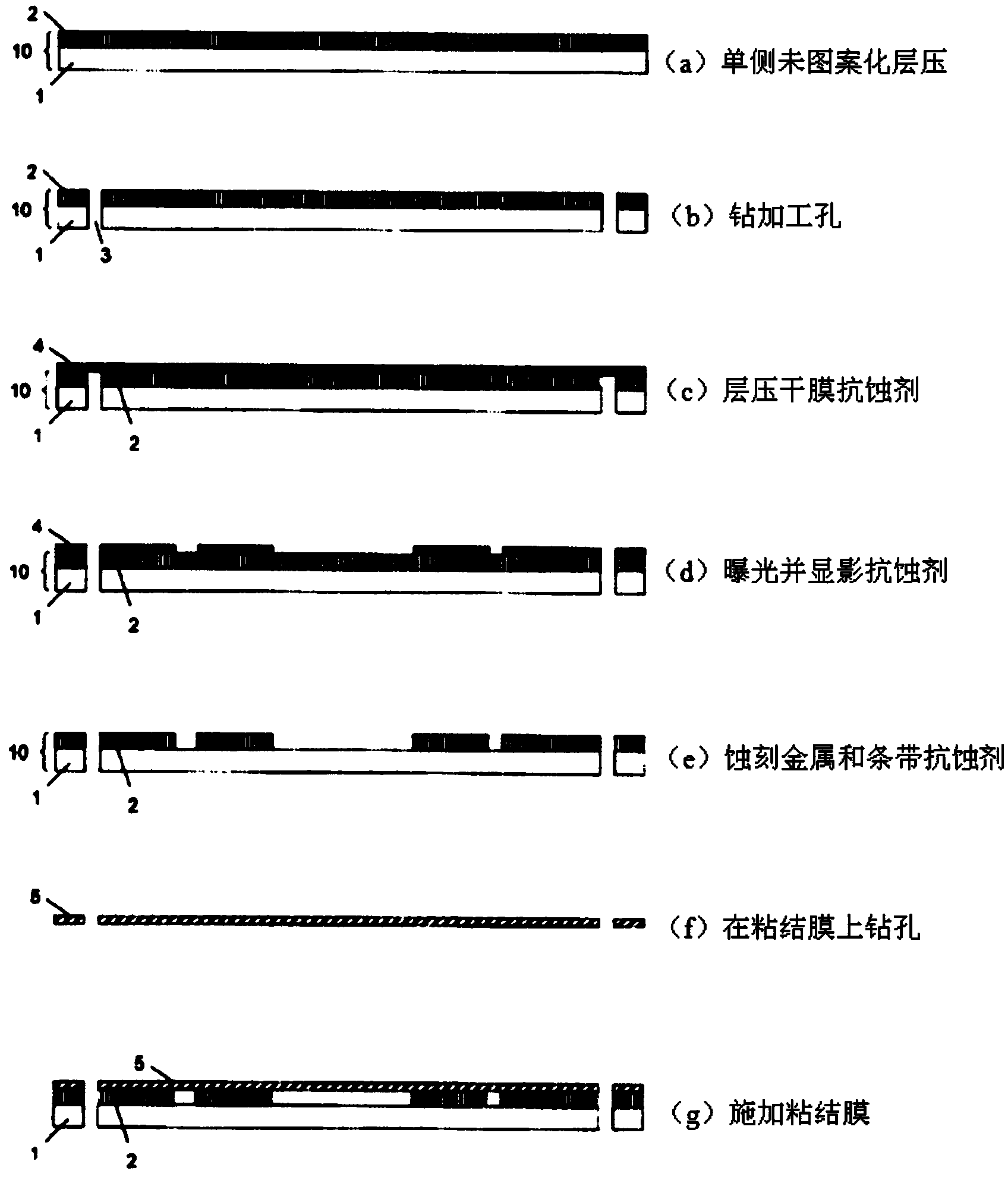
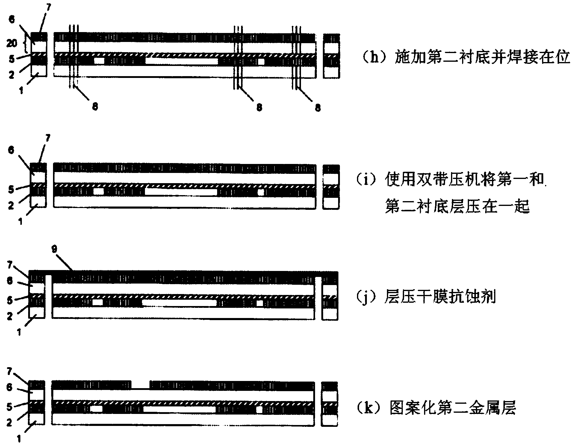
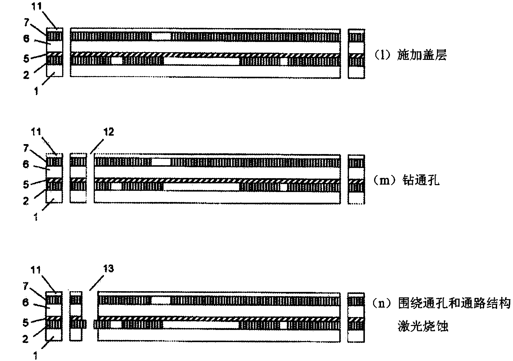
[0051] According to the first embodiment, the method for producing a multi-layer flexible PCB of any length is summarized as the following steps (a) to (k), hereinafter referred to Figure 1 to Figure 3 to describe.

[0052] It should be understood that, for simplicity, Figure 1 to Figure 8 The topology obtained by laminating the first and second substrates 10, 20 is not shown, but each layer is illustrated as a plane. For example, in practice the adhesive film 5 introduced below would be partially reflowed to partially planarize the topology of the patterned conductive layer, and the layer overlying the topology would bend to fit the topology; for simplicity, in It is not shown in the figure.

[0053] The method according to the first embodiment starts with (a) a first pre-lamination substrate 10 of suitable length comprising an unpatterned continuous metal conductive layer 2 on a continuous unpatterned insulator layer 1 . Such substrates 10 are well known to the skilled ...


PUM


Abstract

A method of manufacturing a multiple conductor layer flexible circuit board (PCB) of arbitrary length takes at least first 10 and second 20 flexible PCBs, each comprising at least one conductor layer and an insulator layer, and laminates these PCBs together using a double belt press 50 as a continuous process. At least the conductor layer of the first PCB is a patterned conductor layer; further conductor layers may either be patterned before or after lamination. The first and second PCBs may be double sided carrying two conductor layers and the lamination may include bondfilm 5 between PCBs. The double belt press may include isobaric and / or isochoric regions 51-56 and provide heat and pressure cycles, and the central area of the press may have a higher temperature / pressure that the entrance or exit areas. The first and second PCBs may have alignment means comprising rows of holes. In addition, the method may also be used with three PCBs being laminated together, or with two PCBs and an additional conductor layer laminated together. The first and second PCBS may be welded together prior to lamination.

Description

technical field [0001] The present invention relates to a method of manufacturing a flexible circuit. More particularly, the present invention relates to a method suitable for fabricating multilayer flexible circuits of any length. Background technique [0002] Flexible circuit boards (PCBs) are known and typically comprise a thin flexible electrically insulating layer (e.g. polyester, polyimide, thermoplastic) over which is provided a patterned electrically conductive layer (e.g. copper) . A further protective cover layer may be placed over the conductive layer to protect the conductive layer, the cover layer having apertures to provide electrical access to the conductive layer. [0003] A single-sided PCB with a single conductive layer on one side of the flexible insulating layer can be fabricated by: laminating together layers of copper and polyimide; depositing a resist coating on said copper layer; The printing method patterns the resist layer; etches the resist laye...

Claims


Application Information

Patent Timeline
IPC IPC(8): H05K3/46
CPCH05K2203/1545H05K3/4638H05K2203/068H05K2201/09063B32B2457/08H05K3/4635H05K2203/167B32B37/1027H05K3/4617H05K3/462B30B5/06H05K1/0393H05K3/4611H05K1/0298H05K3/4644H05K1/115H05K3/06H05K3/064
Inventor 飞利浦·约翰斯顿
Owner TRACKWISE DESIGNS
Why Eureka
Try Eureka