Light emitting diode source and manufacturing method thereof and backlight source with light emitting diode source

A technology of light-emitting diodes and backlights, which is applied in the field of backlights and backlights of liquid crystal display devices. It can solve the problems of long optical path, insufficient light intensity, and poor uniformity, and achieve the effect of good uniformity of light emission.

Inactive Publication Date: 2014-11-19
BEIJING BOE OPTOELECTRONCIS TECH CO LTD
View PDF20 Cites 0 Cited by
  • Summary
  • Abstract
  • Description
  • Claims
  • Application Information

AI Technical Summary

Problems solved by technology

[0004] The inventor finds that there are at least the following problems in the prior art: as image 3 As shown, since the refractive index of the package 14 is higher than that of air, the light 9 emitted from the light-emitting diode light-emitting chip 15 will disperse to both sides when it exits the upper surface of the package 14, and the closer to the side the light 9 is dispersed. At the same time, since the reflectivity increases with the increase of the incident angle, the ratio of the light 9 that is closer to the side (that is, the larger the incident angle) is reflected back into the package 14 is larger, and the ratio of the outgoing The smaller the angle is, until the incident angle is greater than the critical angle, the light 9 is completely reflected; in addition, the optical path of the light 9 emitted from the side is long, and the energy loss is relatively large
Due to the above reasons, the relative intensity of the light 9 emitted from the upper surface of the package 14 is as follows: Figure 4 As shown, as the light output angle (referring to the angle between the light emitted from the package 14 and the vertical direction) increases, it decreases, that is, the light 9 emitted by the LED light source 13 has a high middle intensity and low intensity on both sides, and poor uniformity Thereby also can cause the illuminating uniformity difference of backlight source (although the position of corresponding light-emitting diode light source 13 sides on the light guide plate 11 is subjected to the illumination of two light-emitting diode light sources 13 simultaneously, but as Figure 4 As shown, when the exit angle is 60 degrees, the relative light intensity has been reduced to 0.4, even if superimposed, the light intensity in the middle cannot be reached)

Method used


Image

  • Light emitting diode source and manufacturing method thereof and backlight source with light emitting diode source
  • Light emitting diode source and manufacturing method thereof and backlight source with light emitting diode source
  • Light emitting diode source and manufacturing method thereof and backlight source with light emitting diode source

Examples


Embodiment 1

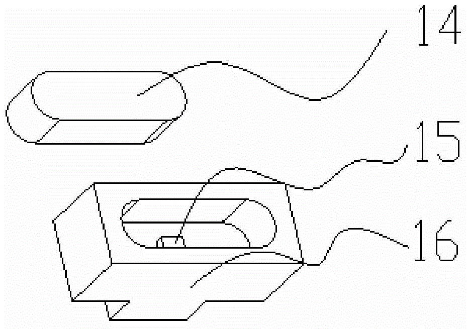
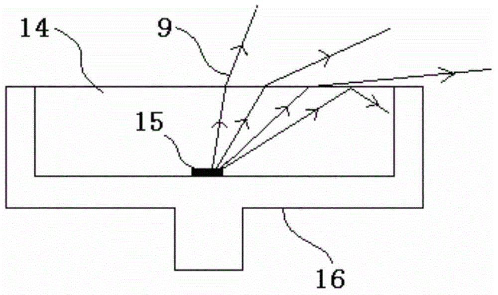
[0048] An embodiment of the present invention provides a light emitting diode light source, such as Figure 5 with Image 6 As shown, it includes: an elongated light-emitting cup 16; a light-emitting diode light-emitting chip 15 arranged at the bottom of the light-emitting cup 16; member 14; a light uniform sheet 17 made of polyethylene on the upper surface of the encapsulation member 14.

[0049] The light uniform sheet 17 has a thickness of 0.1-0.2 mm, and its upper surface has a plurality of triangular prism structures (light uniform structures) 81 on both sides along its length direction (that is, the length direction of the LED light source). These triangular prism structures 81 Arranged side by side perpendicular to the length direction, the bottom of each triangular prism structure 81 is downward and connected to the upper surface of the light uniform sheet 17, and the apex opposite to the bottom is upward.

[0050]Preferably, among the triangular prism structures 81 ...

Embodiment 2

[0053] An embodiment of the present invention provides a light emitting diode light source, such as Figure 8 As shown, it has a structure similar to that of the LED light source in Embodiment 1. The difference is that there is no light uniform sheet 17 , and the above-mentioned triangular prism structure 81 is directly located on the upper surface of the package 14 at both sides along the length direction.

Embodiment 3

[0055] An embodiment of the present invention provides a light emitting diode light source, such as Figure 9 , Figure 10 , Figure 11 As shown, it has a structure similar to that of the LED light source in Embodiment 1. The difference is that there is no triangular prism structure on the upper surface of the light uniform sheet along the length direction, but has a light uniform surface (light uniform structure) 82, and the light uniform surface 82 is inclined downward from the middle to the side along the length direction. Specifically, the light uniform surface 82 can be a plane (such as Figure 9 shown), convex (such as Figure 10 shown), concave (such as Figure 11 Shown) and other forms (such as the combination of various surfaces).

[0056] The light uniform surface 82 acts as the right side of the right triangular prism structure 81 in the first embodiment, thereby improving the light uniformity and overall brightness of the LED light source. However, in order t...


PUM

PropertyMeasurementUnit
Thicknessaaaaaaaaaa

Abstract

The invention provides a light emitting diode source and a manufacturing method thereof and a backlight source with the light emitting diode source, belongs to the technical field of backlight sources of liquid crystal display devices, and solves the problem that an existing light emitting diode source is poor in light emitting uniformity. The light emitting diode source comprises a light emitting cup, fluorescent particles and a light emitting diode chip arranged in the light emitting cup. The light emitting diode source further comprises a light uniformizing structure arranged at the position higher than the light emitting diode chip. The light uniformizing structure comprises two light uniformizing surfaces arranged on the light emitting diode chip and along the length direction of the light emitting diode source. The light uniformizing surfaces extend diagonally and downwardly from the middle to the side along the light emitting diode source.

Description

[0001] This application requires the divisional application of the Chinese patent application submitted to the China Patent Office on September 27, 2010, with the application number 201010294536.0, and the title of the invention is "Light-emitting diode light source and its manufacturing method, and a backlight source with the same", the entire content of which Incorporated in this application by reference. technical field [0002] The invention relates to the technical field of backlight sources of liquid crystal display devices, in particular to a light-emitting diode light source, a manufacturing method thereof, and a backlight source thereof. Background technique [0003] Light-emitting diode (LED) light sources have been used more and more widely because of their advantages such as low power consumption, long life, and fast response speed. For example, in the light-emitting diode backlight of a liquid crystal display device, such as figure 1 As shown, there are a plura...

Claims


Application Information

Patent Timeline
IPC IPC(8): F21S8/00F21V19/00F21V5/02G02F1/13357F21Y101/02
Inventor 孙海威刘佳蔡斯特
Owner BEIJING BOE OPTOELECTRONCIS TECH CO LTD
Why Eureka
Try Eureka