Display substrate, display panel, display and fabrication methods thereof

A technology for display substrates and display panels, used in semiconductor/solid-state device manufacturing, electrical solid-state devices, semiconductor devices, etc., can solve the problem of accelerating the three-phase line pinning of printing ink, aggravating the "coffee ring", and decreasing the uniformity of the film in the pixel, etc. It can reduce the complexity of the preparation process and the production cost, improve the uniformity of light emission, and achieve the effect of good uniformity of light emission.

Inactive Publication Date: 2018-08-03
GUANGDONG JUHUA PRINTING DISPLAY TECH CO LTD
View PDF5 Cites 7 Cited by
  • Summary
  • Abstract
  • Description
  • Claims
  • Application Information

AI Technical Summary

Problems solved by technology

[0005] However, the preparation process of the pixel boundary layer with a double-layer structure is complicated and the preparation cost is high. At the same time, the hydrophilic-hydrophobic interface accelerates the pinning of the three-phase line of the printing ink, which intensifies the formation of "coffee rings" and reduces the uniformity of the film in the pixel.
In addition, the current manufacturing process of the pixel defining layer can only obtain a very thin layer of lyophobic pixel defining layer on the top surface, and the lower part of the pixel defining layer is lyophilic, so that the ink pin point 141 is relatively small during the drying process. High, it is easy to make more ink functional materials accumulated on the side wall of the pixel defining layer, which not only reduces the uniformity of the light-emitting film in the pixel pit, but also is not conducive to the uniform deposition of subsequent functional inks, and aggravates the unevenness of light emission in the pixel. And then affect the performance and life of the device

Method used


Image

  • Display substrate, display panel, display and fabrication methods thereof
  • Display substrate, display panel, display and fabrication methods thereof
  • Display substrate, display panel, display and fabrication methods thereof

Examples


Embodiment Construction

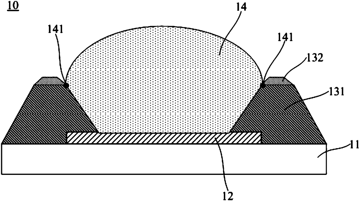
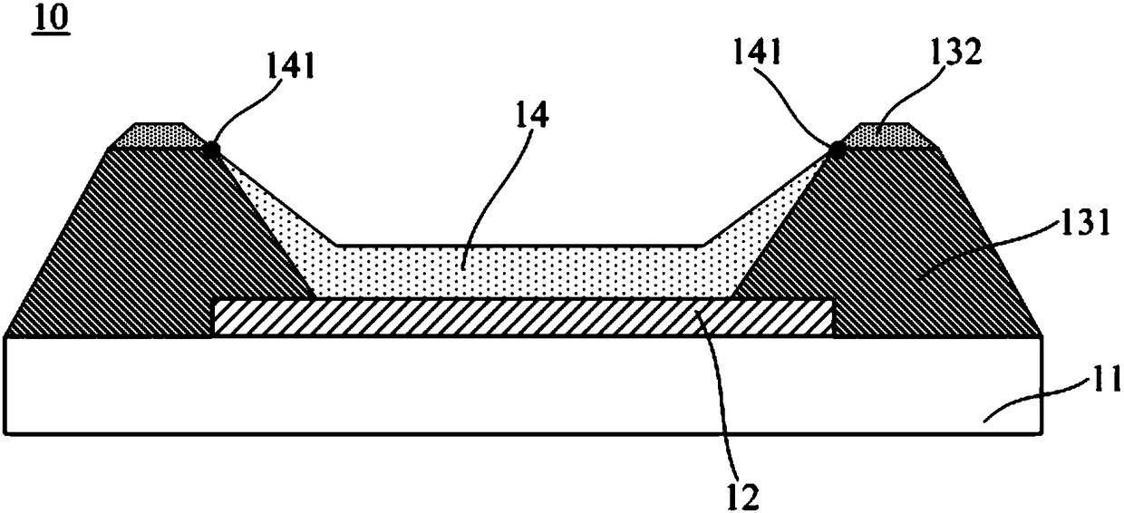
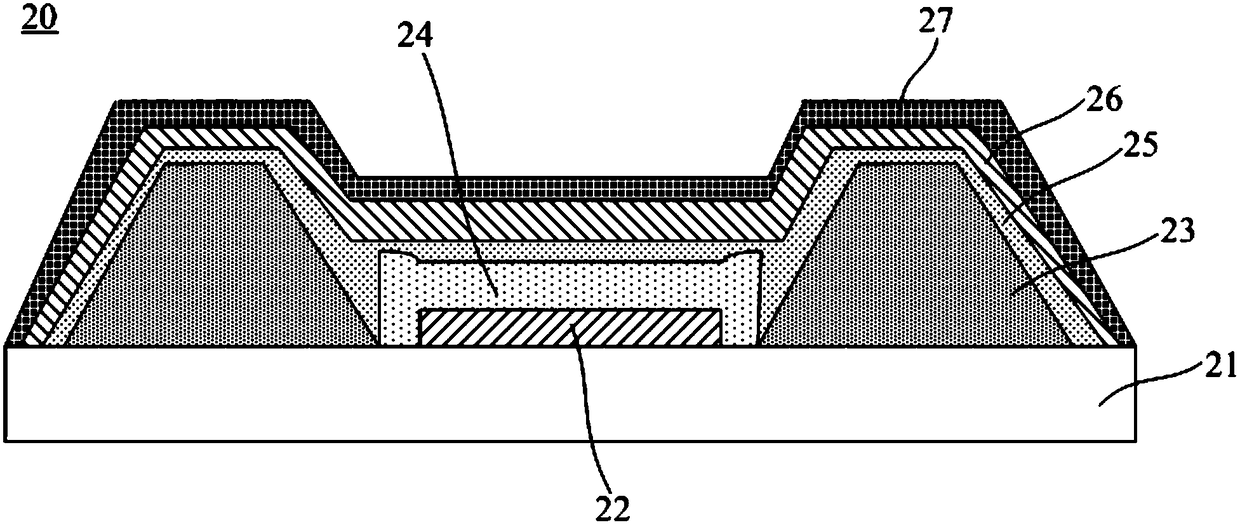
[0038] In order to facilitate the understanding of the present invention, the present invention will be described more fully below with reference to the associated drawings. Preferred embodiments of the invention are shown in the accompanying drawings. However, the present invention can be embodied in many different forms and is not limited to the embodiments described herein. On the contrary, these embodiments are provided to make the understanding of the disclosure of the present invention more thorough and comprehensive.

[0039] It should be noted that when an element is referred to as being “disposed on” or “located on” another element, it may be directly on the other element or there may be an intervening element. When an element is referred to as being "connected to" another element, it can be directly connected to the other element or intervening elements may also be present.

[0040] Unless otherwise defined, all technical and scientific terms used herein have the s...


PUM

PropertyMeasurementUnit
Thicknessaaaaaaaaaa

Abstract

The invention relates to a display substrate, a display panel, a display and fabrication methods thereof. The display substrate comprises first electrodes and a pixel defining layer, wherein the firstelectrodes and the pixel defining layer are arranged on a substrate, the pixel defining layer is arranged between adjacent first electrodes, and gaps are reserved between the first electrodes and thepixel defining layer. Since the gaps are reserved between the first electrodes and the pixel defining layer, pinning points of light-emitting functional ink can be effectively reduced by adjusting distance between the first electrodes and the pixel defining layer, the light-emitting functional ink is further prevented from being accumulated on a wall of the pixel defining layer, current leakage caused by thin film incontinuity of the light-emitting functional layer at an edge of the pixel defining layer is prevented, and the light-emitting uniformity of the display panel or the display can befurther effectively improved; and meanwhile, by the display substrate, the fabrication process complexity and the production cost of the pixel defining layer can be reduced.

Description

technical field [0001] The invention relates to the field of display technology, in particular to a display substrate, a display panel, a display and a manufacturing method thereof. Background technique [0002] Compared with the current mainstream LCD, OLED, as a new third-generation flat panel display technology, has the characteristics of active light emission, simple structure, wide viewing angle, fast response, energy saving, light and thin, and bendable, etc., and has been widely researched and applied. [0003] At present, the commercial application of OLED mainly adopts evaporation technology, but evaporation technology requires relatively expensive vacuum equipment, low material utilization rate, and relatively high production cost, resulting in a disadvantage in market price competition. Solution processing technology, especially inkjet printing technology, has the advantages of simple operation, non-contact, no mask, low equipment cost, high material utilization r...

Claims


Application Information

Patent Timeline
IPC IPC(8): H01L27/32H01L51/56
CPCH10K59/122H10K71/135H10K71/00
Inventor 董婷
Owner GUANGDONG JUHUA PRINTING DISPLAY TECH CO LTD
Why Eureka
Try Eureka