Flat pin-free packaging body
A flat leadless, packaged body technology, applied in the direction of electric solid devices, semiconductor devices, semiconductor/solid device components, etc., to avoid the limitations of the base process and ensure the quality of the effect
- Summary
- Abstract
- Description
- Claims
- Application Information
AI Technical Summary
Problems solved by technology
Method used
Image
Examples
Embodiment Construction
[0013] In order to better understand the spirit of the present invention, it will be further described below in conjunction with some preferred embodiments of the present invention.
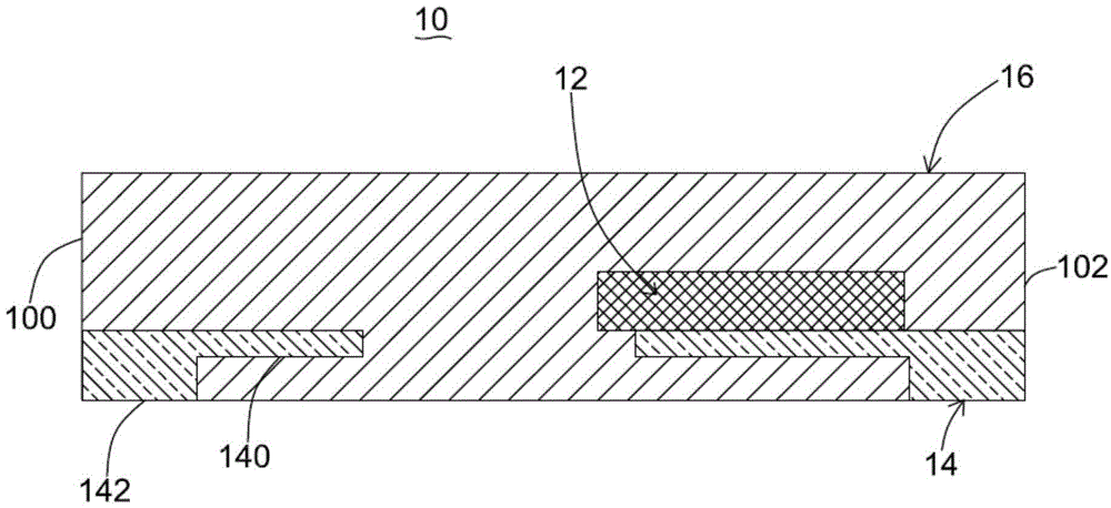
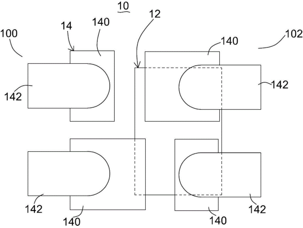
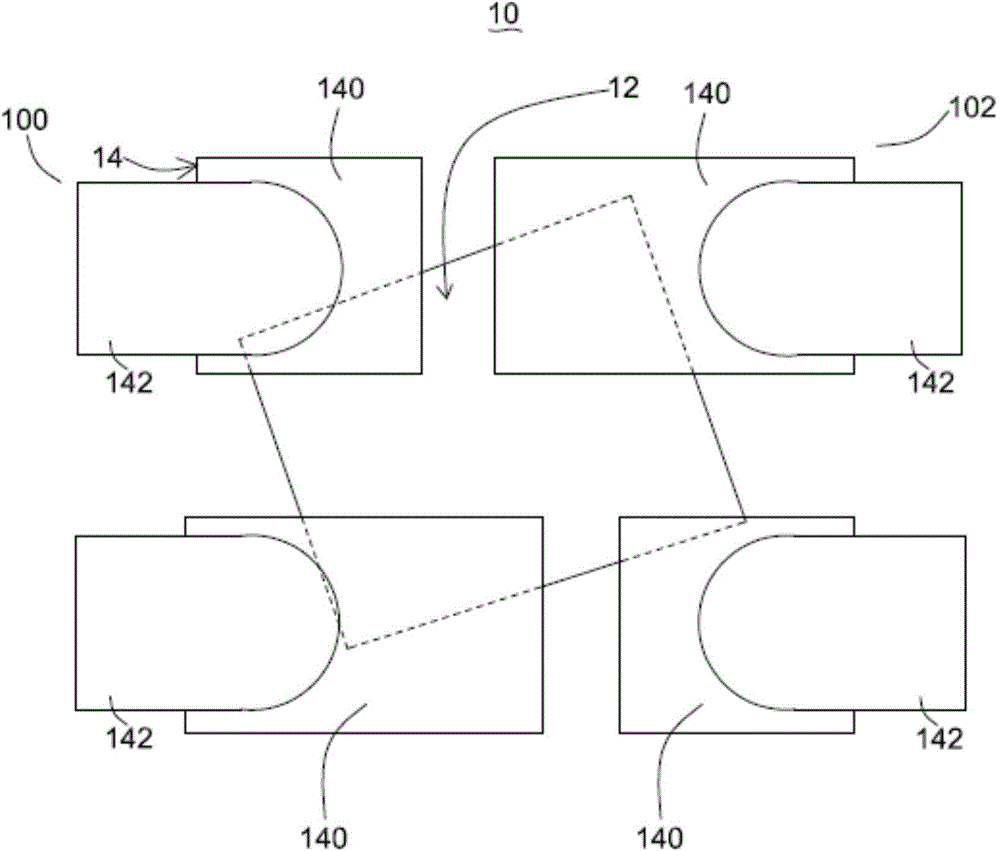
[0014] For chips with a small size such as less than 2mm×2mm, limited by the existing pedestal technology, a package without a pedestal can be used. That is, the chip is mounted directly on the pins. However, due to considerations of multiple design factors, sometimes the chip cannot be located in the center of the entire package but is biased to one side. In this way, according to the symmetrical arrangement of pins designed according to traditional design rules, there may be a situation where a row of pins cannot touch the chip, and a large area of the corresponding chip will be suspended. Due to the large area of the chip suspended in the air, during the wire bonding operation, the chip cannot be bonded due to the unstable loading of the chip.
[0015] Embodiments of the present inventio...
PUM
 Abstract
Description
Claims
Application Information
 - R&D Engineer
- R&D Manager
- IP Professional
- Industry Leading Data Capabilities
- Powerful AI technology
- Patent DNA Extraction
Browse by: Latest US Patents, China's latest patents, Technical Efficacy Thesaurus, Application Domain, Technology Topic, Popular Technical Reports.
© 2024 PatSnap. All rights reserved.Legal|Privacy policy|Modern Slavery Act Transparency Statement|Sitemap|About US| Contact US: help@patsnap.com


