Method for Improving Reliability of Semiconductor Devices in Interconnection Processes

A semiconductor and reliability technology, applied in the field of interconnection, can solve the problems of reduced reliability of semiconductor devices and easy damage of intermetallic dielectrics, and achieve the effects of improving device yield, improving performance, and reducing damage

Active Publication Date: 2017-03-15
SEMICON MFG INT (SHANGHAI) CORP
View PDF4 Cites 0 Cited by
  • Summary
  • Abstract
  • Description
  • Claims
  • Application Information

AI Technical Summary

Problems solved by technology

[0007] In view of the shortcomings of the prior art described above, the purpose of the present invention is to provide a method for improving the reliability of semiconductor devices in the interconnection process, which is used to solve the problem of the previous interconnection structure under the top-level metal interconnection structure in the prior art. The low-k value intermetallic dielectric is easily damaged, and further solves the problem of reduced reliability of semiconductor devices in the interconnection process

Method used


Image

  • Method for Improving Reliability of Semiconductor Devices in Interconnection Processes
  • Method for Improving Reliability of Semiconductor Devices in Interconnection Processes
  • Method for Improving Reliability of Semiconductor Devices in Interconnection Processes

Examples


Embodiment Construction

[0029] Embodiments of the present invention are described below through specific examples, and those skilled in the art can easily understand other advantages and effects of the present invention from the content disclosed in this specification. The present invention can also be implemented or applied through other different specific implementation modes, and various modifications or changes can be made to the details in this specification based on different viewpoints and applications without departing from the spirit of the present invention.

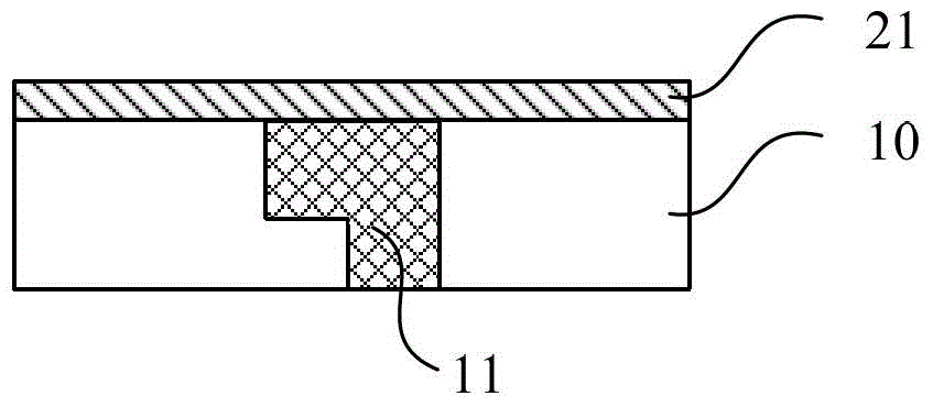
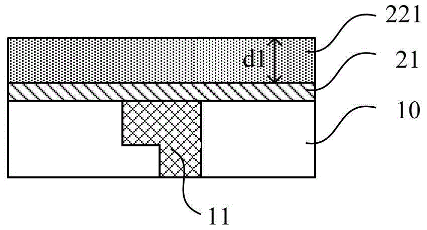
[0030] see Figure 1 to Figure 3 . It should be noted that the illustrations provided in the following specific embodiments are only schematically illustrating the basic idea of ​​the present invention, and only the components related to the present invention are shown in the drawings rather than the number and shape of components in actual implementation. and size drawing, the type, quantity and proportion of each component can be c...


PUM


Abstract

The invention provides a method for improving reliability of a semiconductor device of an interconnection process. According to the invention, a top layer interconnection structure-based dielectric substance layer containing a first plasma enhance oxide (PEOX) layer and a second PEOX layer arranged on the first PEOX layer is formed by two steps, wherein the energy and deposition rate for forming the first PEOX layer are lower than the energy and deposition rate for forming the second PEOX layer, so that compared with the second PEOX layer, the first PEOX layer has the higher compactness and higher pressure stress. Because a metal tensile stress is exerted on an ultra-low k value-contained intermetallic dielectric substance of the previous interconnection structure directly under the top layer interconnection structure for top layer interconnection structure preparation, the first PEOX layer has the higher pressure stress to eliminate the metal tensile stress well, thereby reducing the damages on the ultra-low k value-contained intermetallic dielectric substance due to the metal tensile stress. Therefore, the leakage current is reduced and performances of puncture voltage and electromigration and the like of the device can be improved, thereby improving performances of electrical performance testing and reliability of the device and enhancing the device yield.

Description

technical field [0001] The invention belongs to the interconnection technology of semiconductor manufacturing process in the field of semiconductor manufacturing process, and relates to a method for improving the reliability of semiconductor devices in the interconnection process, in particular to a related preparation method of a top-level interconnection structure in the semiconductor device interconnection process. Background technique [0002] With the continuous reduction of the size of semiconductor devices, the interconnection structure is becoming narrower and narrower, and the space between the metal wiring is gradually shrinking, so the intermetal dielectric (intermetal dielectric) used to isolate the metal wiring -metal dielectric, IMD) is also becoming thinner, resulting in the possibility of adverse interaction or crosstalk between metal wiring. [0003] It has been found that reducing the dielectric constant (k) of the intermetallic dielectric used to isolate t...

Claims


Application Information

Patent Timeline
Patent Type & Authority Patents(China)
IPC IPC(8): H01L21/768H01L21/316
CPCH01L21/7688
Inventor 白凡飞赵婧宋兴华
Owner SEMICON MFG INT (SHANGHAI) CORP
Why Eureka
Try Eureka