Divergent sensing apparatus and manufacturing method thereof

A technology of a sensing device and a manufacturing method, which can be applied to microstructure devices, manufacturing microstructure devices, decorative arts, etc., can solve problems such as high cost, large fingerprint sensor or chip area, etc.

Inactive Publication Date: 2014-12-03
MOREVALUED TECHNOLOGY CO LTD
View PDF7 Cites 11 Cited by
  • Summary
  • Abstract
  • Description
  • Claims
  • Application Information

AI Technical Summary

Problems solved by technology

For example, if the sensing array has 100×100 sensing elements, it will have a sensing area of ​​about 5mm×5mm. If the surrounding analog and digital circuits are added, the area of ​​the entire fingerprint sensor or chip will be quite large. , making the cost quite high

Method used


Image

  • Divergent sensing apparatus and manufacturing method thereof
  • Divergent sensing apparatus and manufacturing method thereof
  • Divergent sensing apparatus and manufacturing method thereof

Examples


Embodiment Construction

[0074] In order to make the object, technical solution and advantages of the present invention clearer, the embodiments of the present invention will be further described in detail below in conjunction with the accompanying drawings. Here, the exemplary embodiments and descriptions of the present invention are used to explain the present invention, but not to limit the present invention.

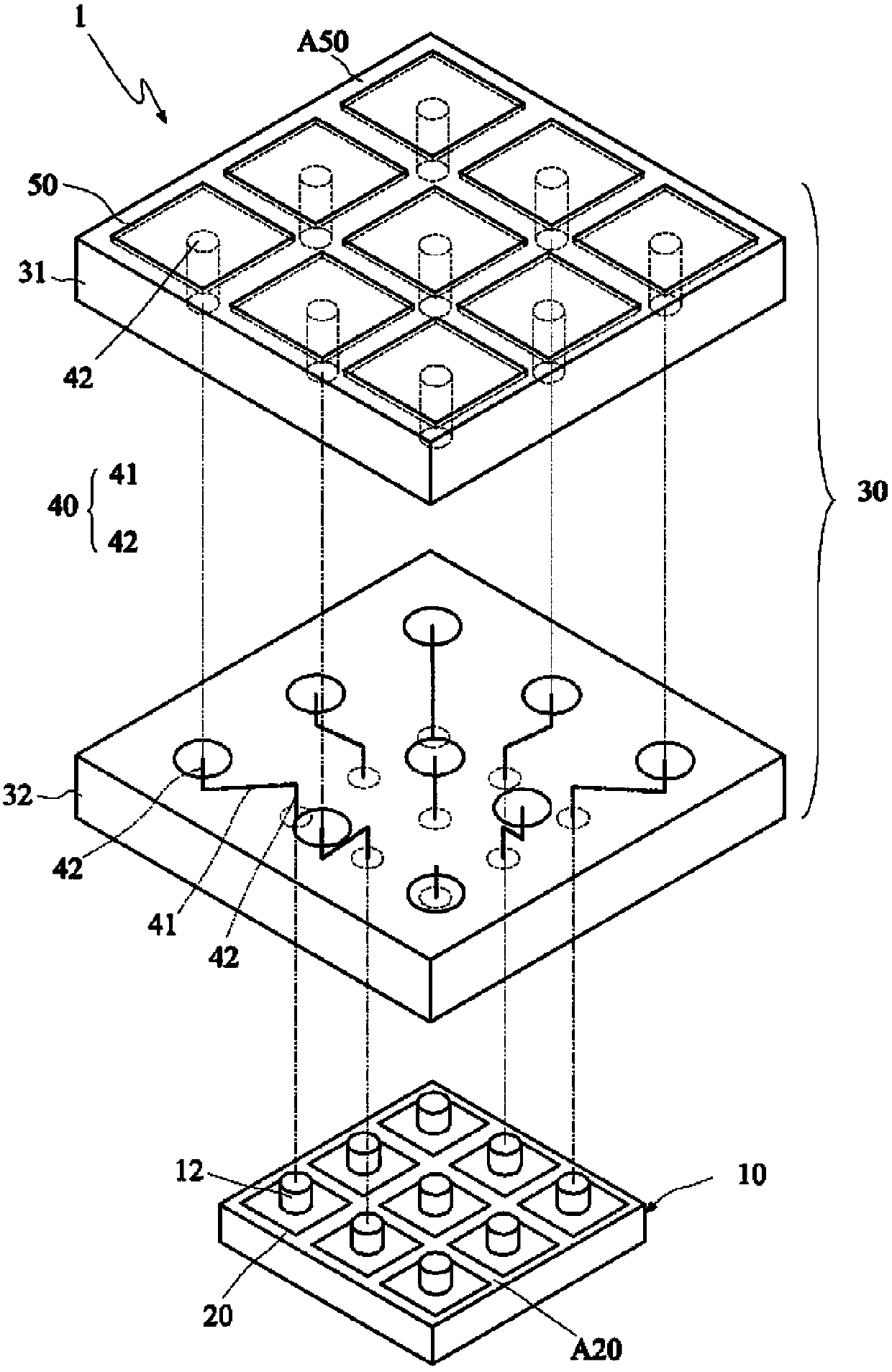
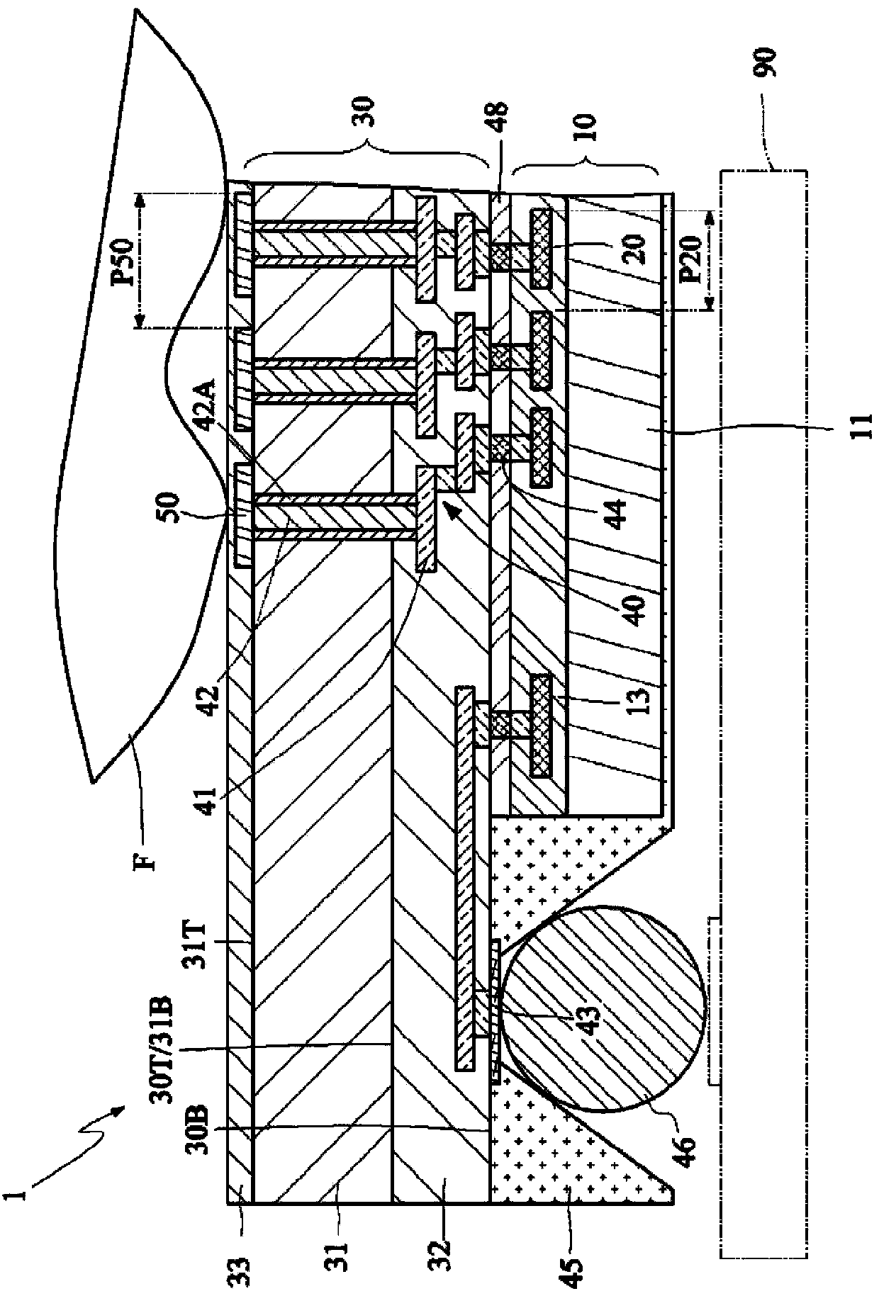
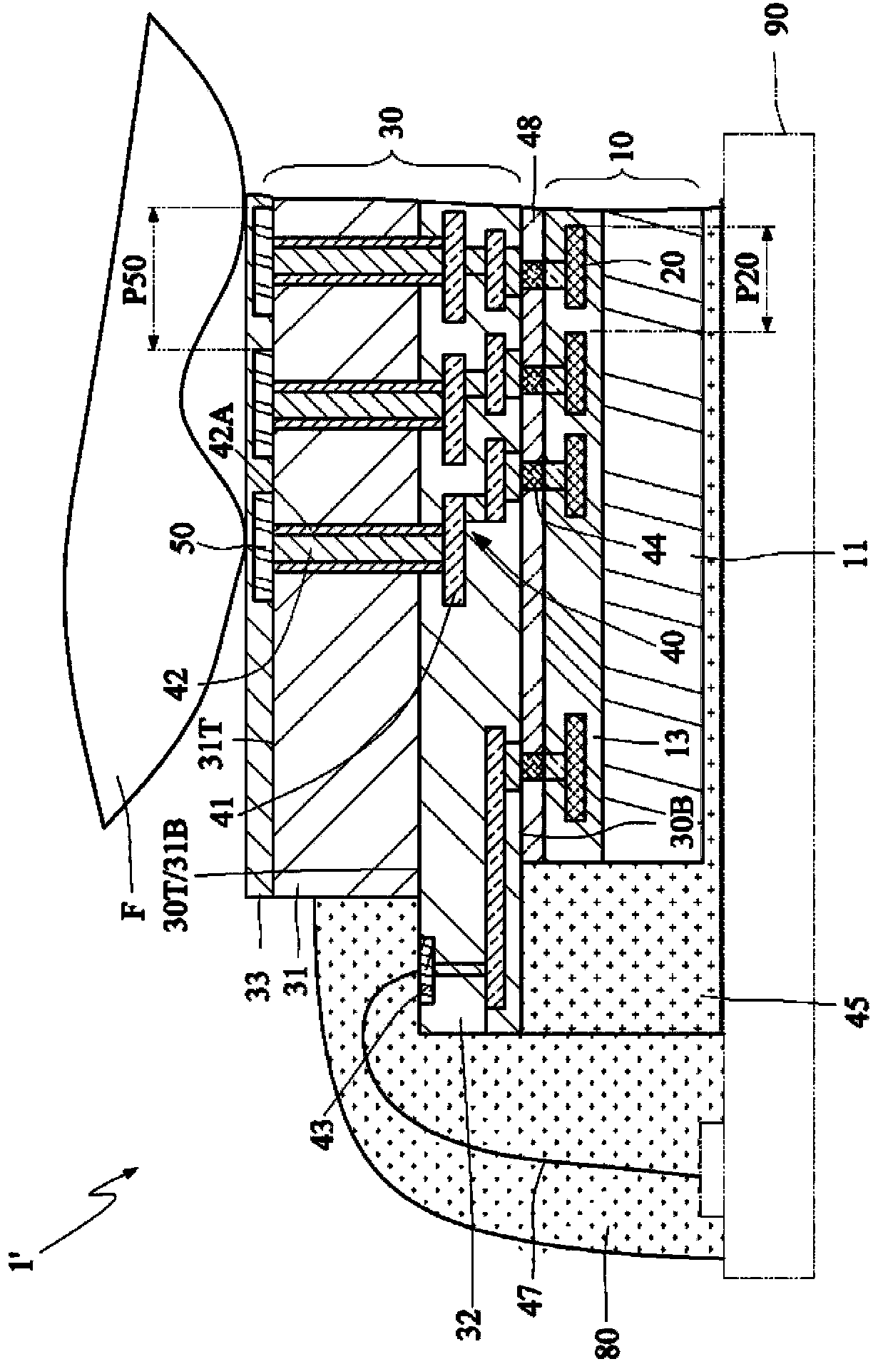
[0075] The concept of the present invention is mainly how to save the IC area covering the sensing circuit and related peripheral processing circuits, so as to save the cost of the area-based fingerprint sensing device. The idea behind the implementation of the present invention is to disassemble the sensing device into a sensing circuit element array (including related peripheral processing circuits as monolithic ICs) and a sensing electrode element array actually in contact with the hand, and make them separately. Because the sensing circuit element array is a complete IC manufacturing pro...


PUM


Abstract

The invention discloses a divergent sensing apparatus and a manufacturing method thereof. The divergent sensing apparatus comprises a lower structural body, an upper structural body, a plurality of divergent lines and a plurality of sensing electrode units, wherein a plurality of sensing circuit units are formed in the lower structural body, the upper structural body is arranged on the lower structural body along a vertical direction; the plurality of divergent lines are formed in the upper structural body and electrically connected with the sensing circuit units. Each divergent line comprises at least one horizontal extending section and at least one vertical extending section which are vertical each other. The plurality of sensing electrodes are formed in the upper structural body, and electrically connected with the divergent lines. The sensing electrode units sense biological characteristics of an organism to generate a plurality of sensing signals which are transmitted to the sensing circuit units through the divergent lines. The sensing circuit units process the sensing signals to obtain a plurality of output signals. The smallest distribution area covering the sensing circuit units is equal to or smaller than the smallest distribution area covering the sensing electrode units.

Description

technical field [0001] The present invention generally relates to a sensing device and a manufacturing method thereof, and in particular to a divergent sensing device and a manufacturing method thereof, as well as applying the sensing device to technologies such as fingerprint sensing. Background technique [0002] Traditional non-optical fingerprint sensing devices, such as electric field / capacitance, thermal sensing, pressure sensing and other fingerprint sensing devices, must sense the texture of the finger, so the sensing area needs to maintain contact with the finger area in order to obtain sufficient sensing accuracy. Taking the electric field / capacitive fingerprint sensor as an example, it has a plurality of sensing elements arranged in an array, and the area occupied by these sensing elements corresponds to the area of ​​the finger one to one. For example, in the design of a fingerprint sensor with a resolution of 500dpi, the pitch of the sensing elements in the sen...

Claims


Application Information

Patent Timeline
Patent Type & Authority Applications(China)
IPC IPC(8): G06K9/20G06K9/00B81C1/00
Inventor 邱立国
Owner MOREVALUED TECHNOLOGY CO LTD
Why Eureka
Try Eureka