Electric response reflection device and preparation method thereof
A reflective device, electrical response technology, applied in instruments, optics, nonlinear optics, etc., can solve the problems of inflexibility, single color, single, etc.
- Summary
- Abstract
- Description
- Claims
- Application Information
AI Technical Summary
Problems solved by technology
Method used
Image
Examples
Embodiment 1
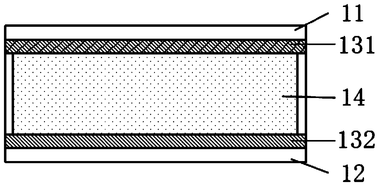
[0027] An electrical response reflective device, the preparation method of which comprises the following steps:
[0028] S1. Take the first light-transmitting conductive substrate and the second light-transmitting conductive substrate. In this embodiment, the first light-transmitting conductive substrate and the second light-transmitting conductive substrate are light-transmitting conductive glass substrates;
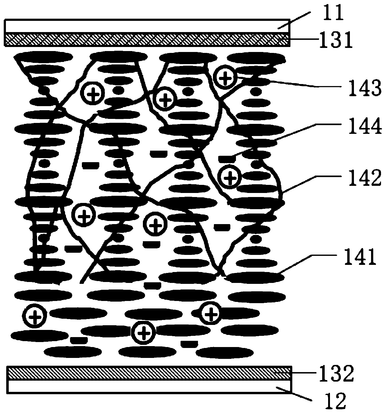
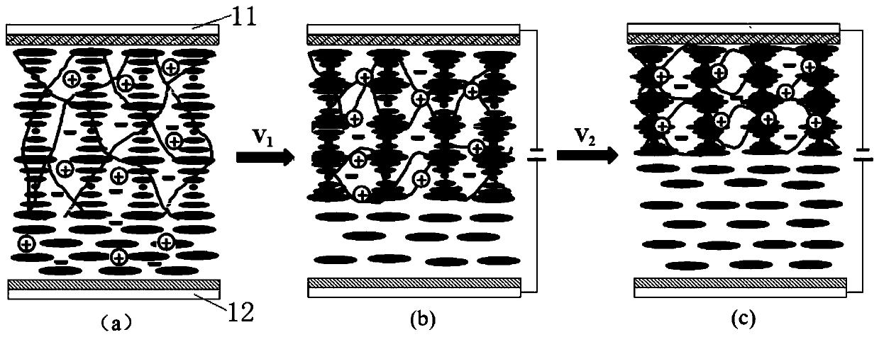
[0029] S2. Weigh polyvinyl alcohol and dissolve it in deionized water, add 1 mass part (1 g per mass) of photoinitiator Irgacure-651 to mix, prepare a solution with a concentration of 5 wt%, and stir at 60°C until completely dissolved Then spin-coat on a surface of the first light-transmitting conductive substrate to prepare an alignment layer material layer, control the film thickness by controlling the spin-coating speed and time to be about 75 nanometers, and then rub parallel alignment to form the first parallel alignment layer; Weigh polyvinyl alcohol and dissolve ...
Embodiment 2
[0049] This example is basically the same as Example 1, except that the liquid crystal mixture includes 80 parts by mass of negative liquid crystal MLC-2079, 16.5 parts by mass of chiral polymerizable liquid crystal monomer HCM-006 and 3 parts by mass of polymerizable Liquid crystal monomer HCM-002; the alignment layer material in the first parallel alignment layer is doped with 0.5 parts by mass of photoinitiator Irgacure-819; each part by mass is 1 g.
Embodiment 3
[0051] This example is basically the same as Example 1, except that the liquid crystal mixture includes 85 parts by mass of negative liquid crystal HNG-30400-200, 8 parts by mass of chiral polymerizable liquid crystal monomer HCM-006, and 5 parts by mass of Polymerizable liquid crystal monomer HCM-008; in addition, in this embodiment, the material of the alignment layer is polyimide; the material of the alignment layer in the first parallel alignment layer is doped with 2 parts by mass of photoinitiator Irgacure-369; 1g.
PUM
| Property | Measurement | Unit |
|---|---|---|
| Thickness | aaaaa | aaaaa |
Abstract
Description
Claims
Application Information


