Electric fuse structure and method for forming same, semiconductor device and method for forming same
一种电熔丝、半导体的技术,应用在半导体器件、半导体/固态器件制造、半导体/固态器件零部件等方向,能够解决形成方法单一等问题,达到形成方法简单、结构新颖的效果
- Summary
- Abstract
- Description
- Claims
- Application Information
AI Technical Summary
Problems solved by technology
Method used
Image

Examples
no. 1 example
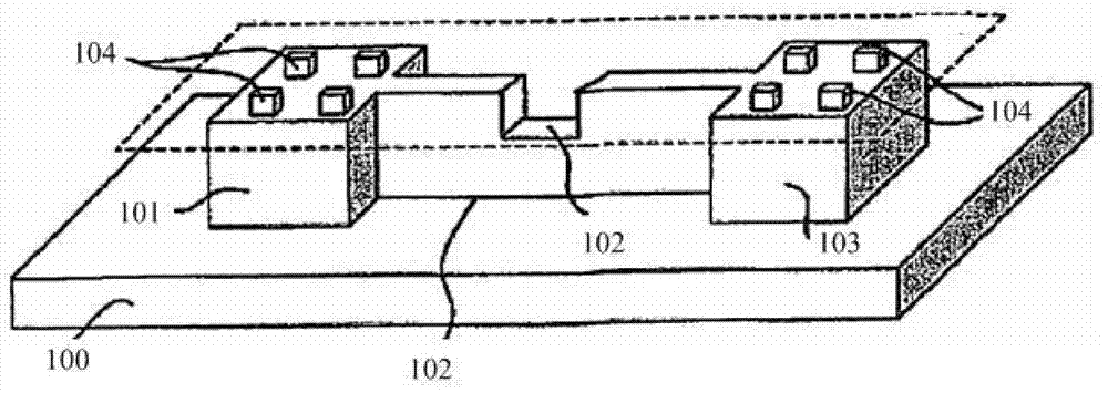
[0077] In the first embodiment of the present invention, the inventor provides a method and structure for forming an electric fuse when forming a gate-all-around transistor.
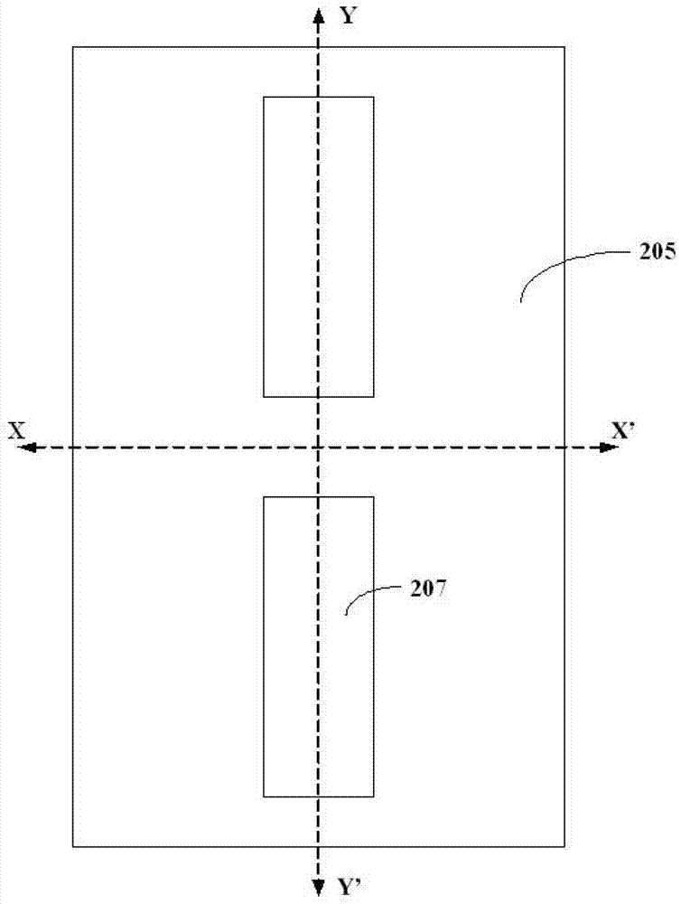
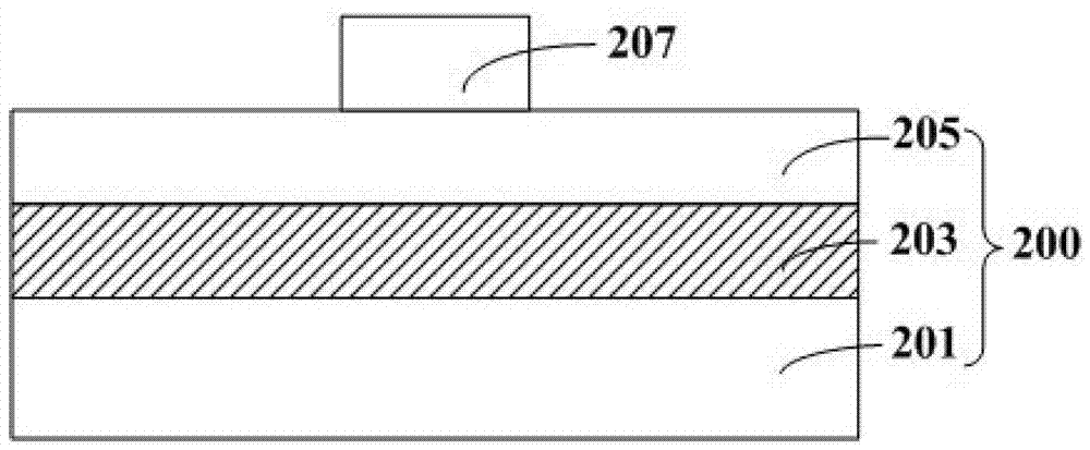
[0078] Please refer to Figure 2A , 2B , 2C, where, Figure 2A It is a schematic top view structure diagram of the formation process of the semiconductor device according to the first embodiment of the present invention, Figure 2B for Figure 2A Schematic diagram of the cross-sectional structure along the X-X' direction; Figure 2C for Figure 2A Schematic diagram of the cross-sectional structure along the Y-Y' direction.
[0079] It should be noted that, in order to facilitate the understanding of the present invention, in the embodiments of the present invention, the schematic cross-sectional structure along the X-X' direction only shows the structure on the cross-section.
[0080] Provide a semiconductor-on-insulator substrate (SOI) 200 including a first region I and a second region II, wherein...
no. 2 example
[0149] Different from the first embodiment, in the second embodiment of the present invention, a method for forming an electric fuse structure is provided. The electric fuse structure does not necessarily have to be parasitic in the formation step of the gate-enclosed transistor, and can be independently Formation of electrical fuse structures on nanowires on semiconductor substrates.
[0150] Please refer to Figure 16 , provide a semiconductor-on-insulator substrate, the semiconductor-on-insulator substrate includes a back substrate 301, a buried oxide layer 303 covering the surface of the back substrate 301, and a top semiconductor layer (not shown) covering the surface of the buried oxide layer 303 mark); etch the top semiconductor layer to form a suspended nanowire 305f, which is used to form an electric fuse structure including a cathode 323, an anode 325 and a fusing region; doping at both ends of the nanowire 305 The cathode 323 and the anode 325 forming the electric ...
no. 3 example
[0164] Different from the first and second embodiments of the present invention, in the third embodiment of the present invention, the electric fuse structure is formed at the same time as the FinFET. Moreover, the process of the fin field effect transistor in the first region is divided into a process of forming the high-k gate dielectric layer before (HK First) and a process of forming the high-k gate dielectric layer after (HK Last). In the third embodiment of the present invention, the electric fuse structure is formed during the process of forming the high-k gate dielectric layer first.
[0165] Please refer to Figure 17 and Figure 18 ,in, Figure 17 It is a schematic diagram of the three-dimensional structure of the formation process of the semiconductor device, Figure 18 for Figure 17 Schematic diagram of the cross-sectional structure along the A-A1 direction.
[0166] Firstly, a semiconductor substrate 400 is provided, the semiconductor substrate 400 includes ...
PUM
 Abstract
Description
Claims
Application Information
 - R&D
- Intellectual Property
- Life Sciences
- Materials
- Tech Scout
- Unparalleled Data Quality
- Higher Quality Content
- 60% Fewer Hallucinations
Browse by: Latest US Patents, China's latest patents, Technical Efficacy Thesaurus, Application Domain, Technology Topic, Popular Technical Reports.
© 2025 PatSnap. All rights reserved.Legal|Privacy policy|Modern Slavery Act Transparency Statement|Sitemap|About US| Contact US: help@patsnap.com