

Manufacturing method of solar cell unit
A technology of solar cells and manufacturing methods, which is applied in the direction of electrical components, final product manufacturing, sustainable manufacturing/processing, etc., and can solve problems such as hindering carrier movement and decreasing power generation efficiency
- Summary
- Abstract
- Description
- Claims
- Application Information
AI Technical Summary
Problems solved by technology
Method used
Image

Examples
no. 1 Embodiment approach
[0025] Solar cells are designed in many types. For example, a crystalline Si-based solar cell secures superiority over other types of solar cells by its simple structure and fabrication method, high conversion efficiency, and the like. On the other hand, in order to obtain a higher conversion efficiency in a crystalline Si-based solar cell, it is important to identify the most suitable condition pair for each process unit. Among them, the formation of the surface emitter layer by the photoelectric effect is considered to be a very important element, and it is considered that the following characteristics are preferable.
[0026] However, both the thermal diffusion method and the ion implantation method, which are currently used as general manufacturing methods, are difficult to satisfy the following characteristics at the same time due to their characteristics.
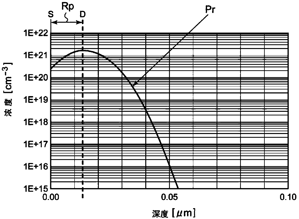
[0027] (1) Shallow junction. Specifically, the internal diffusion potential is brought closer to the surface.
...
no. 2 Embodiment approach
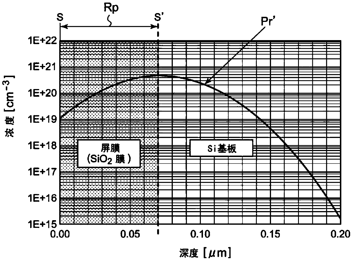
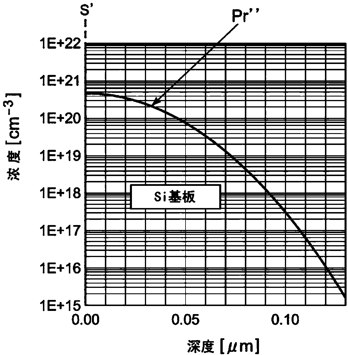
[0052] In this embodiment, the case where an antireflection film is used as a screen film will be described. Image 6 It is a flowchart of the manufacturing method of the solar cell which concerns on 2nd Embodiment. Figure 7 (a)~ Figure 7 (e) is a schematic cross-sectional view of the semiconductor substrate in each step of the method of manufacturing a solar cell according to the second embodiment. In addition, the same code|symbol is attached|subjected to the same structural element or process as 1st Embodiment, and description is abbreviate|omitted suitably.
[0053] First, as Figure 7 As shown in (a), a texture ( Image 6 S10). Then, as Figure 7 As shown in (b), SiN or TiO is formed on the surface of the silicon substrate 10 by a CVD method or the like 2 Equal anti-reflection film 16 ( Image 6 S24). The thickness of the antireflection film 16 is, for example, about 10 to 100 nm. Thus, a solar cell substrate having a p-type (first conductivity type) silicon su...
no. 3 Embodiment approach
[0060] In the present embodiment, an anti-reflection film is used as the panel film, and a case where a contact region is formed in addition to the emitter layer will be described. Figure 8 It is a flowchart of the manufacturing method of the solar cell which concerns on 3rd Embodiment. Figure 9 (a)~ Figure 9 (e) is a schematic cross-sectional view of the semiconductor substrate in each step of the method of manufacturing a solar cell according to the third embodiment. Figure 10 (a)~ Figure 10 (b) is a schematic cross-sectional view of a semiconductor substrate in each step of the method of manufacturing a solar cell according to the third embodiment. In addition, the same code|symbol is attached|subjected to the same structural element and process as each said embodiment, and description is abbreviate|omitted suitably.
[0061] First, as Figure 9 As shown in (a), a texture ( Figure 8 S10). Then, as Figure 9 As shown in (b), SiN or TiO is formed on the surface o...
PUM
 Abstract
Description
Claims
Application Information