A kind of array substrate and its preparation method, display device

An array substrate and peripheral technology, applied in optics, instruments, electrical components, etc., can solve the problem of reducing the aperture ratio of display devices

Active Publication Date: 2017-08-29
HEFEI XINSHENG OPTOELECTRONICS TECH CO LTD +1
View PDF6 Cites 0 Cited by
  • Summary
  • Abstract
  • Description
  • Claims
  • Application Information

AI Technical Summary

Problems solved by technology

[0007] Embodiments of the present invention provide an array substrate, its preparation method, and a display device, which can solve the problem that the common electrode lines reduce the aperture ratio of the display device

Method used


Image

  • A kind of array substrate and its preparation method, display device
  • A kind of array substrate and its preparation method, display device
  • A kind of array substrate and its preparation method, display device

Examples


Embodiment 1

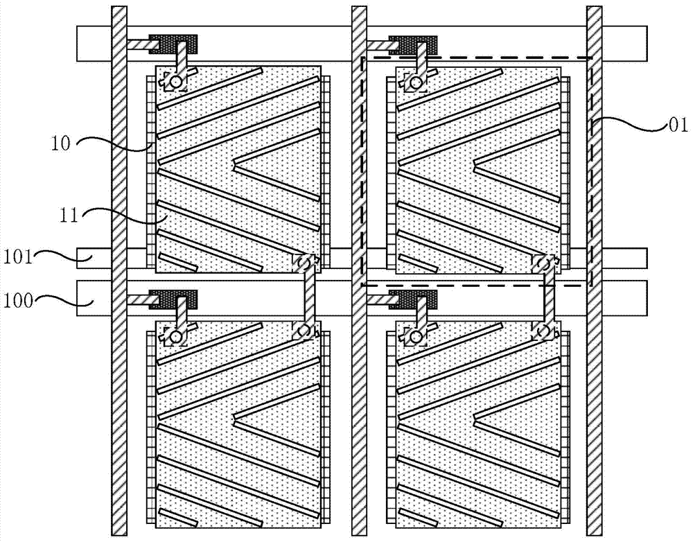
[0054] Such as Figure 3a As shown, the array substrate may further include a plurality of third connection portions 130, arranged between two adjacent pixel units 01 along the second direction, for electrically connecting the common electrodes 10 of the two adjacent pixel units 01 .

[0055] Specifically, the above-mentioned third connecting portion 130 may be made of a transparent conductive material. When the third connection part 130 is made of a transparent conductive material, a via hole (not shown) can be formed on the surface of the pixel electrode 11 at a position corresponding to the third connection part 130, and then a third connection made of a transparent conductive material can be made. The part 130 electrically connects the common electrodes 10 of two adjacent pixel units 01 through the above-mentioned via holes. However, the pixel electrode 11 is also made of transparent conductive material. Therefore, it is also necessary to form an insulating layer betwee...

Embodiment 2

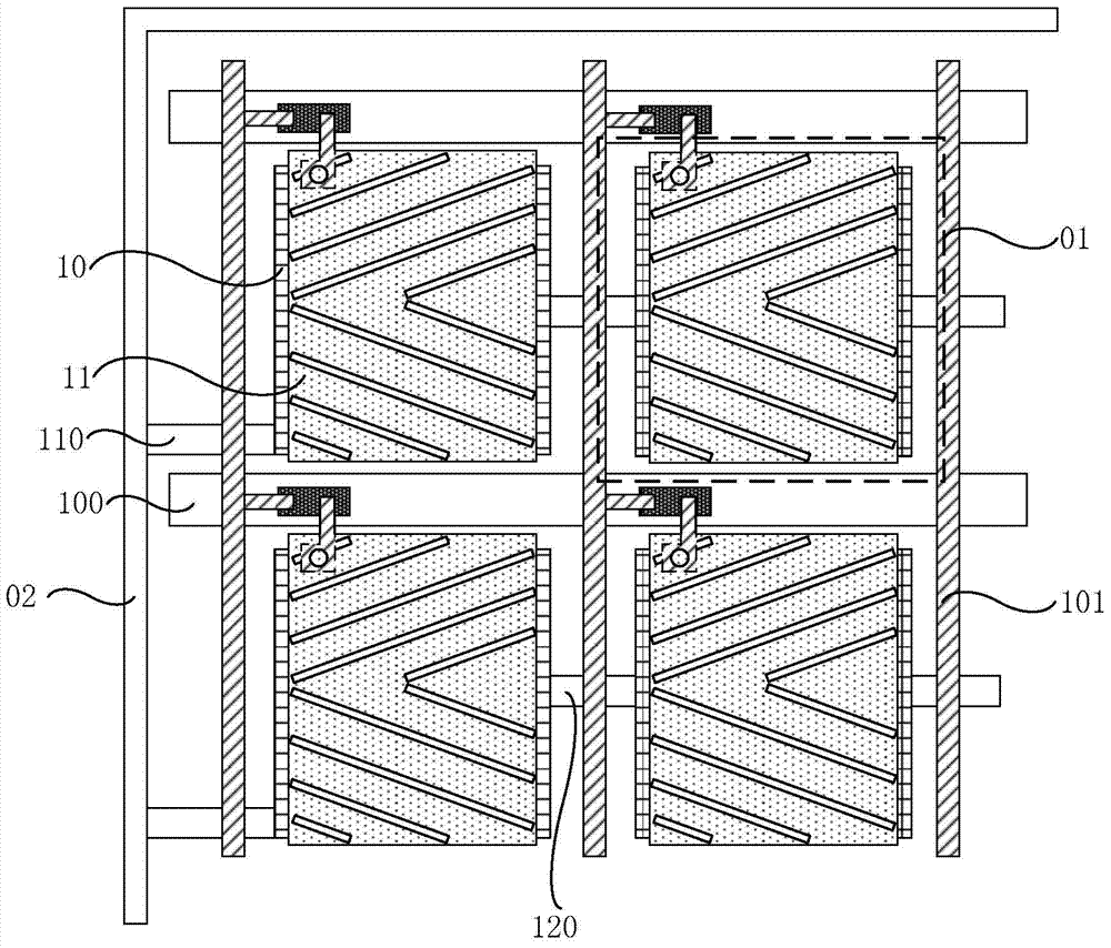
[0064] Such as Figure 4aAs shown, on the basis of Embodiment 1, the array substrate may further include a plurality of fourth connecting parts 140, which are arranged on the peripheral common electrode line 02 and the pixels on the side close to the peripheral common electrode line 02 along the second direction. Between the common electrodes 10 of the unit 01 is used to electrically connect the peripheral common electrode line 02 to the common electrode 10 of the above-mentioned pixel unit 01 .

[0065] Like the third connecting portion 130 in the first embodiment, the fourth connecting portion 140 may also be made of transparent conductive material.

[0066] Alternatively, in order to improve the electrical conductivity of the fourth connecting portion 140, the fourth connecting portion 140 may also be made of a metal material.

[0067] Preferably, in the case where the array substrate includes data lines 101, such as Figure 4b ( Figure 4a sectional view along BB').

...

Embodiment 3

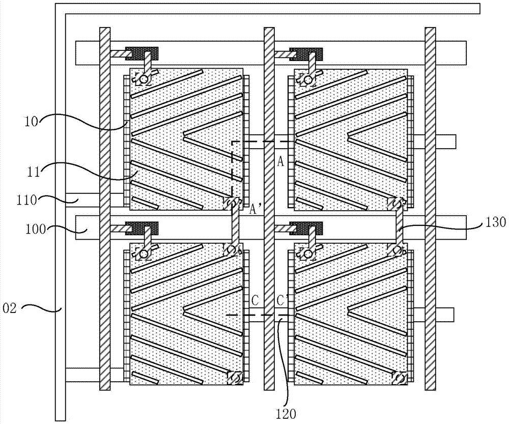
[0091] Such as Figure 7 shown, including:

[0092] S201, such as Figure 8a As shown, a common electrode layer 04 is formed on a base substrate 03 .

[0093] Specifically, the above-mentioned common electrode layer 04 may be made of a transparent conductive material, such as ITO. The common electrode layer 04 may be deposited on the surface of the base substrate 03 by using a magnetron sputtering method.

[0094] S202 , forming a gate metal layer 05 on the surface of the common electrode layer 04 .

[0095] Specifically, the aforementioned gate metal layer 05 may be formed on the surface of the common electrode layer 04 by coating or magnetron sputtering.

[0096] S203, such as Figure 8b shown (where, Figure 8b —8d is edge Figure 3a The cross-sectional view of CC' is described by taking the second connection part 120 as an example, and the manufacturing process of the first connection part 110 can be obtained in the same way), and a layer of photoresist is coated on...


PUM


Abstract

The invention provides an array substrate, a preparation method thereof, and a display device, which relate to the field of display technology and can solve the problem that common electrode lines reduce the aperture ratio of the display device. The array substrate includes a peripheral common electrode line for supplying a common voltage, a plurality of pixel units, and a plurality of first connection parts and second connection parts. Wherein, the first connection portion is disposed along the first direction between the peripheral common electrode line and the common electrode of the pixel unit near the peripheral common electrode line, and electrically connects the peripheral common electrode line to the common electrode. The second connection portion is arranged between the common electrodes of every two adjacent pixel units along the first direction to electrically connect the two adjacent common electrodes.

Description

technical field [0001] The present invention relates to the field of display technology, in particular to an array substrate, a preparation method thereof, and a display device. Background technique [0002] TFT-LCD (Thin Film Transistor Liquid Crystal Display, Thin Film Transistor Liquid Crystal Display), as a flat panel display device, has become more and more popular due to its small size, low power consumption, no radiation and relatively low production cost. It is widely used in the field of high-performance display. [0003] TFT-LCD consists of an array substrate and a color filter substrate. A liquid crystal layer is provided between the array substrate and the color filter substrate, and an electric field is formed in the liquid crystal layer by applying voltages to the pixel electrodes provided on the array substrate and the common electrodes provided on the color filter substrate or the array substrate respectively. Then, the transmittance of light passing throug...

Claims


Application Information

Patent Timeline
Patent Type & Authority Patents(China)
IPC IPC(8): G02F1/1345G02F1/1362
CPCG02F1/136286G02F2201/121G02F1/134372G02F1/13629H01L27/124G02F1/1345H01L27/1259H01L33/42
Inventor 冯伟
Owner HEFEI XINSHENG OPTOELECTRONICS TECH CO LTD
Why Eureka
Try Eureka