Communication device, test system and test method thereof

A technology of a communication device and a test system, applied in the field of communication, can solve the problem of wasting pin resources of a baseband chip, and achieve the effect of saving pin resources and improving system performance

Active Publication Date: 2014-12-17
SPREADTRUM COMM (SHANGHAI) CO LTD
View PDF5 Cites 2 Cited by
  • Summary
  • Abstract
  • Description
  • Claims
  • Application Information

AI Technical Summary

Problems solved by technology

[0005] The present invention solves the problem of wasting pin resources of the baseband chip when testing the target test chip integrated into the baseband chip in the prior art

Method used


Image

  • Communication device, test system and test method thereof
  • Communication device, test system and test method thereof
  • Communication device, test system and test method thereof

Examples


Embodiment 1

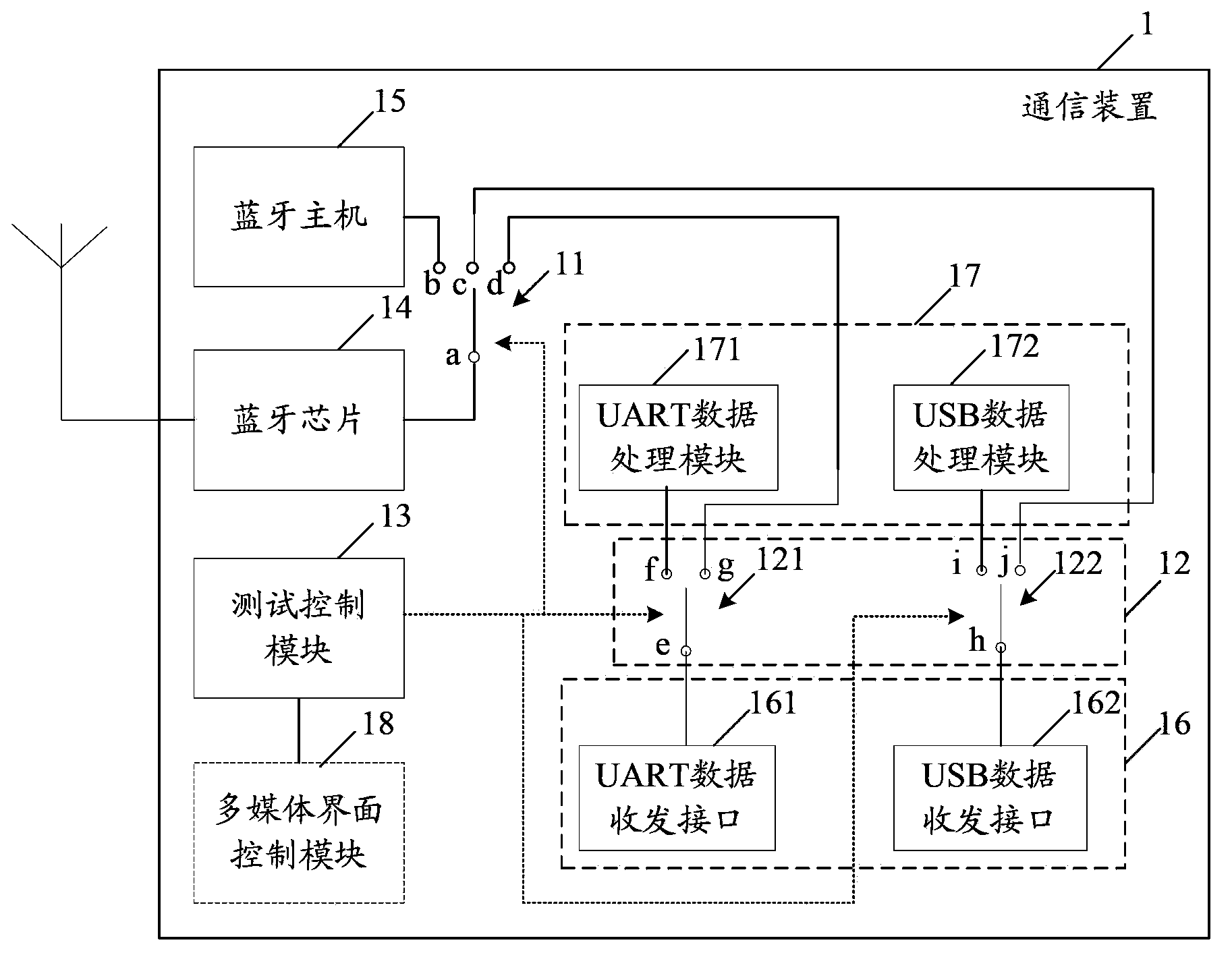
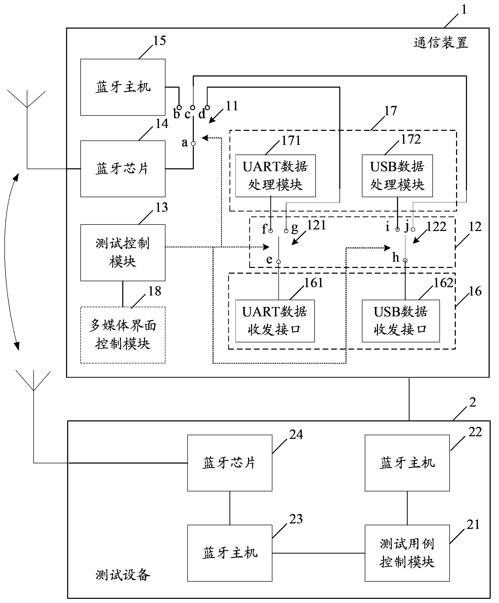
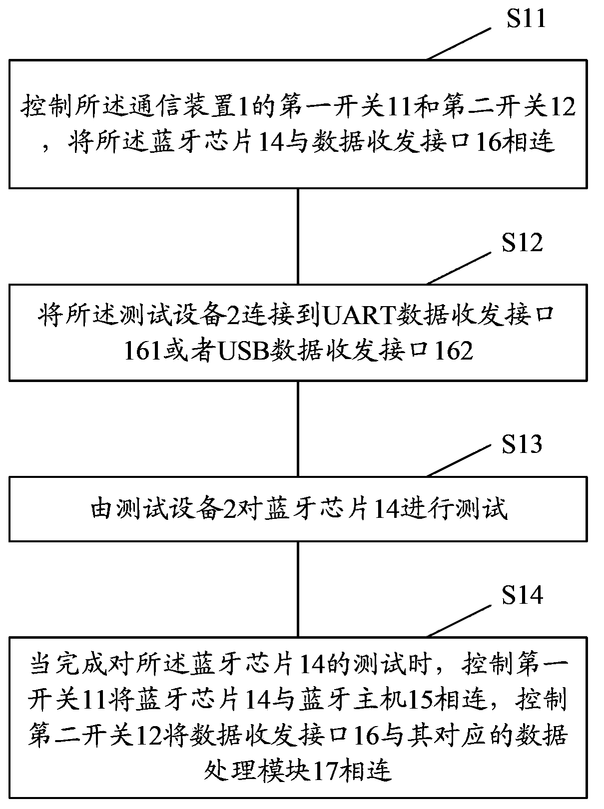
[0044] figure 1Shown is the communication device 1 provided by Embodiment 1 of the present invention. The Bluetooth chip 14 of the communication device 1 is integrated in a baseband chip, and the upper layer processing module of the Bluetooth chip 14 is a Bluetooth host 15 . Described communication device 1 also comprises data transceiving interface 16, and data transceiving interface 16 among the present embodiment is made up of a UART data transceiving interface 161 and a USB data transceiving interface 162, and their corresponding data processing modules 17 are UART data processing modules respectively. Module 171 and USB data processing module 172. Usually, a communication device (such as a mobile phone) has a tail jack for charging, debugging, data transmission, software upgrade, etc. of the communication device. The UART data transceiving interface 161 and the USB data transceiving interface 162 in this embodiment are usually implemented through the tail socket of the c...

Embodiment 2

[0057] Such as Figure 4 As shown, it is a schematic structural diagram of a communication device 3 according to Embodiment 2 of the present invention. The communication device 3 includes: a Bluetooth chip 14, a Bluetooth host 15, a data transceiver interface 16 and a corresponding data processing module 17, a first switch 11, a second A switch 12 , a test control module 13 , a format conversion module 19 and a third switch 20 . It can be seen that the difference from the communication device 1 in Embodiment 1 is that a format conversion module 19 and a third switch 20 connected thereto are added between the first switch 11 and the second switch 12 . It can be seen that the first switch in Embodiment 1 can directly control the connection between the target test chip and the data transceiver interface; while the first switch in this embodiment needs to be indirectly controlled by the format conversion module and the third switch. Controlling the connection between the target t...

Embodiment 3

[0067] Such as Figure 7 As shown, it is a schematic structural diagram of a communication device 4 according to Embodiment 3 of the present invention, including: a Bluetooth chip 14, a Bluetooth host 15, a data transceiver interface 16 and its corresponding data processing module 17, a first switch 11, a second switch 12, Test the control module 13 , the format conversion module 19 and the third switch 20 . It can be seen that this embodiment is an implementation mode after combining Embodiment 1 and Embodiment 2, that is, the Bluetooth chip 14 can be directly connected to the data transceiver interface 16, and can also communicate with the data transceiver interface 19 via the format conversion module 19. The interface 16 is indirectly connected. Specifically, when the bluetooth chip 14 and the test equipment 2 send and receive commands, instructions or data formats that are the same, the first switch 11 is controlled to connect the node a to the node d', and then the secon...


PUM


Abstract

The present invention provides communication device, test system and test method thereof, the communication device comprising: a baseband chip, and a target test chip, an upper processing module on the target test chip, at least one data receiving and transmitting interface and a data processing module thereof, a first switch, a second switch and a test control module integrated in the baseband chip, wherein the first switch is used for achieving connection between the target test chip and the data receiving and transmitting interface or the upper processing module; the second switch is used for achieving connection between the data receiving and transmitting interface and the data processing module or the target test chip; the test control module is used for controlling the first and second switches to connect the data receiving and transmitting interface with the target test chip, so that the communication device is suitable for testing the target test chip. The technical solution of the present invention does not need additional test pins while testing the target chip, saves resources for the communication device and reduces cost.

Description

technical field [0001] The invention relates to the technical field of communication, in particular to a communication device, a test system and a test method thereof. Background technique [0002] With the development of semiconductor technology, integrated chips came into being. An integrated chip is a chip that integrates multiple chip functions into one chip. Its birth enables electronic products to achieve more functions with a smaller volume. For example, the baseband chip in the existing communication device integrates the functions of many peripheral chips, making the appearance of the communication device thinner and smaller. [0003] Among them, the most common is the application of integrating the Bluetooth chip into the baseband chip, so that the communication device can complete the baseband processing function and the Bluetooth function at the same time with only one baseband chip installed, without the need to install a separate Bluetooth chip, which saves en...

Claims


Application Information

Patent Timeline
Patent Type & Authority Applications(China)
IPC IPC(8): H04B17/00
CPCH04M1/24H04M2250/02G01R31/3177H04L43/50
Inventor 顾祥新崔世军罗亮亮张明伟
Owner SPREADTRUM COMM (SHANGHAI) CO LTD
Why Eureka
Try Eureka