Printed circuit board

A technology of printed circuit boards and boards, which is applied in the direction of printed circuits, printed circuit components, electrical connection printed components, etc., and can solve problems such as impedance discontinuity

Inactive Publication Date: 2014-12-17
HONG FU JIN PRECISION IND (SHENZHEN) CO LTD +1
View PDF0 Cites 5 Cited by
  • Summary
  • Abstract
  • Description
  • Claims
  • Application Information

AI Technical Summary

Problems solved by technology

[0002] At present, in the design of printed circuit boards, when a chip mounted on a printed circuit board in a quad flat package (QFP) transmits a differential signal, the impedance may be discontinuous due to the influence of the transmission line, thereby causing signal Integrity issues

Method used


Image

  • Printed circuit board
  • Printed circuit board
  • Printed circuit board

Examples


Embodiment Construction

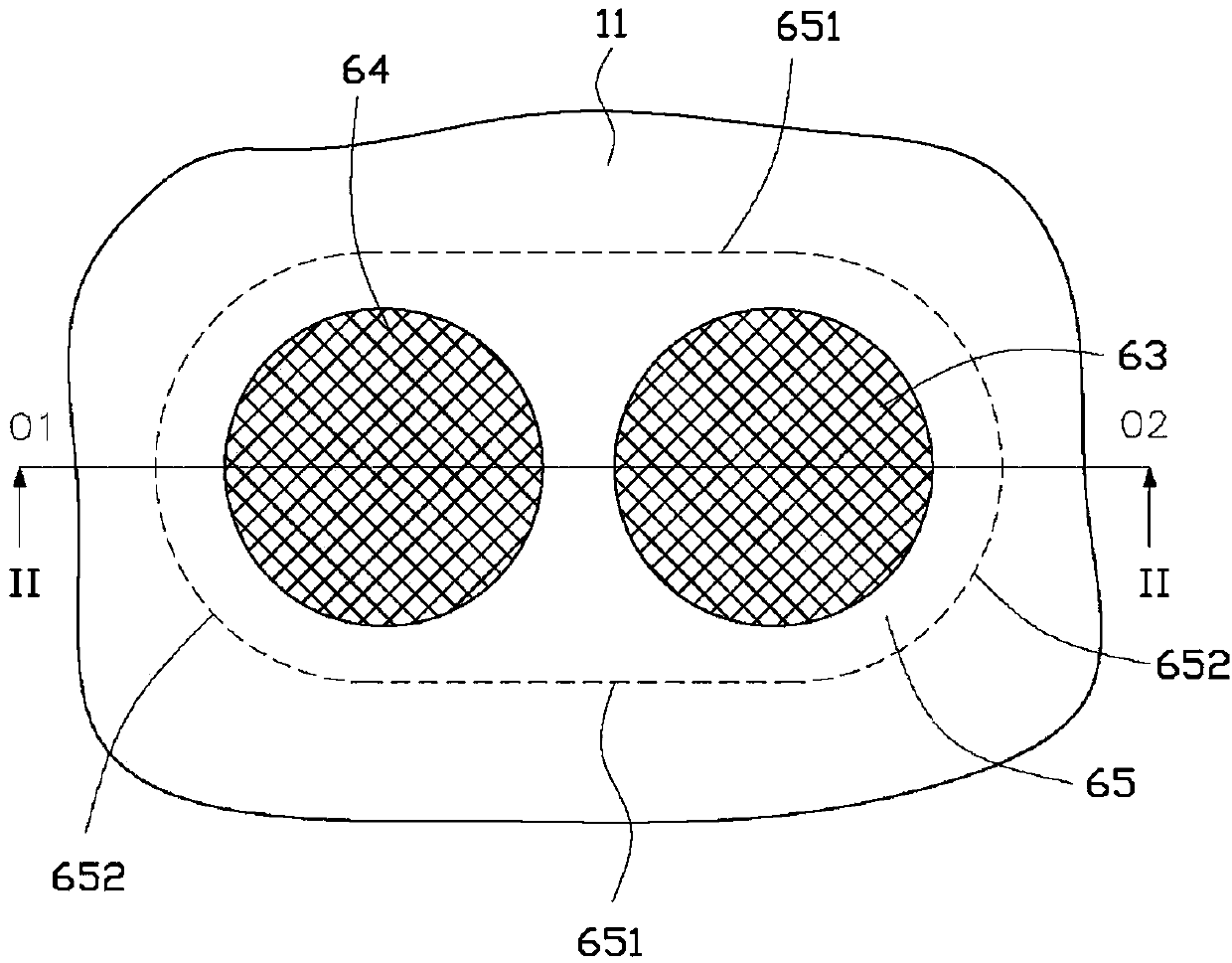
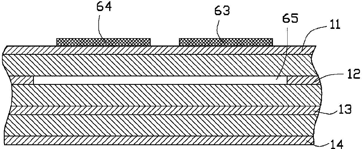
[0012] Please refer to figure 1 and figure 2 , The printed circuit board of the present invention includes a board body 1 . The board body 1 includes a top layer 11 , a bottom layer 14 and several reference layers arranged between the top layer 11 and the bottom layer 12 . In this embodiment, the board body 1 is a four-layer printed circuit board, and the reference layer includes a power layer 12 and a signal layer 13 . The top layer 11 is a signal layer, and the bottom layer 14 is a ground layer.

[0013] Several welding pads are provided on the board body 1 , and in this embodiment, two welding pads 63 and 64 are taken as an example for illustration. The solder pads 63 and 64 are disposed on the top layer 11 of the board body 1 to be connected to the signal transmission lines on the top layer 11 . The pads 63 and 64 are used to connect a pair of differential pins of a quad flat package (QFP) chip, so as to transmit differential signals between the QFP chip and the compo...


PUM


Abstract

A printed circuit board comprises a board body, wherein the board body comprises a top layer, a bottom layer and a plurality of reference layers, wherein the reference layers are arranged between the top layer and the bottom layer; the board body is provided with a first bonding pad and a second bonding pad; the first bonding pad and the second bonding pad are arranged on the top layer of the board body, are connected with signal transmission lines on the top layer and are connected with a pair of differential pins of a square flat packaging chip; an avoidance hole is formed in the reference layer which is close to the first bonding pad and the second bonding pad, and is positioned right below the first bonding pad and the second bonding pad; and orthographic projections of the first bonding pad and the second bonding pad on the reference layer which is close to the first bonding pad and the second bonding pad are positioned in a range of the avoidance hole. By the printed circuit board, discontinuity of impedance can be effectively reduced, and the signal transmission quality is improved.

Description

technical field [0001] The invention relates to a printed circuit board. Background technique [0002] At present, in the design of printed circuit boards, when a chip mounted on a printed circuit board in a quad flat package (QFP) transmits a differential signal, the impedance may be discontinuous due to the influence of the transmission line, thereby causing signal Integrity issues. Contents of the invention [0003] In view of the above, it is necessary to provide a printed circuit board that can effectively reduce the impedance discontinuity, so as to improve the quality of signal transmission. [0004] A printed circuit board, comprising a board body, the board body includes a top layer, a bottom layer and several reference layers arranged between the top layer and the bottom layer, a first welding pad and a second soldering pad are arranged on the board body The first and second pads are arranged on the top layer of the board and connected to the signal transmissio...

Claims


Application Information

Patent Timeline
Patent Type & Authority Applications(China)
IPC IPC(8): H05K1/02H05K1/11
CPCH05K1/0225H05K1/025H05K1/111Y02P70/50
Inventor 张云何苗
Owner HONG FU JIN PRECISION IND (SHENZHEN) CO LTD
Why Eureka
Try Eureka