Lc snubber circuit

A snubber circuit and snubber diode technology, applied in electrical components, high-efficiency power electronics conversion, output power conversion devices, etc., can solve problems such as narrow power supply voltage range, achieve low switching voltage stress, reduce peak voltage stress, reduce Effect of Small Conduction Loss

Inactive Publication Date: 2014-12-24
ABB RES LTD
View PDF4 Cites 6 Cited by
  • Summary
  • Abstract
  • Description
  • Claims
  • Application Information

AI Technical Summary

Problems solved by technology

Some of the LC buffers developed can improve the performance [7]–[9], but they are limited to a narrow supply voltage range

Method used


Image

  • Lc snubber circuit
  • Lc snubber circuit
  • Lc snubber circuit

Examples


Embodiment Construction

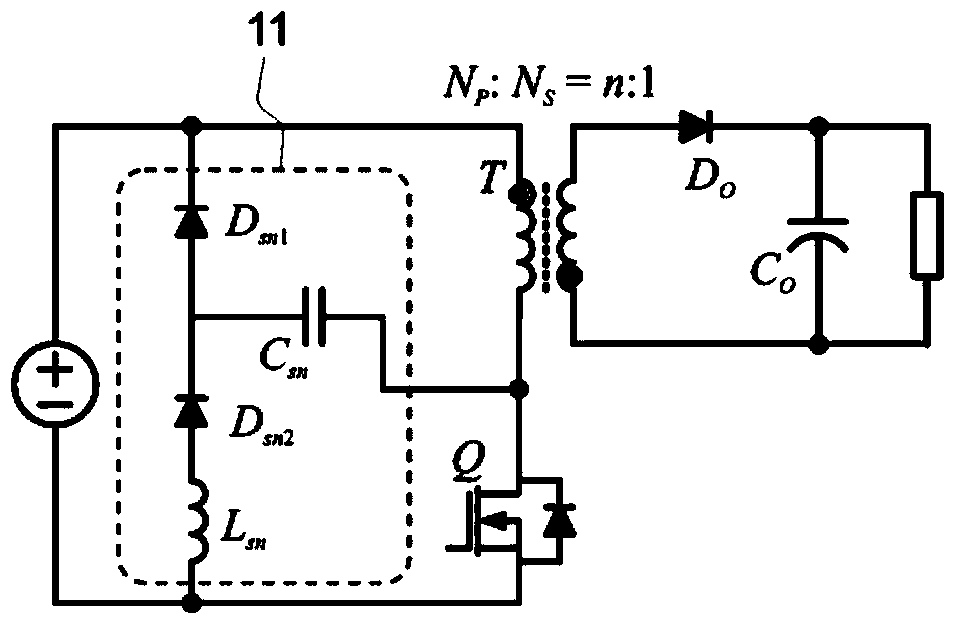
[0021] Next, install the flyback converter such as Figure 1a The principle of operation of the illustrated conventional LC buffer is discussed in more detail. Circulating currents causing additional conduction losses were also investigated. Figure 2a to Figure 2c show Figure 1a Exemplary voltage waveforms and exemplary current waveforms for the buffer shown in . exist Figure 2a The magnetizing current I of the transformer T is shown in Lm and leakage current I lkg , and the current I through the switching device Q Q ;exist Figure 2b The voltage V across the switching device Q is shown in Q and in the snubber capacitor C sn The voltage on V Csn ;exist Figure 2c is shown through the snubber diode D sn1 current I Dsn1 and through the snubber diode D sn2 current I Dsn2 .

[0022] Figure 3a to Figure 3e show Figure 1a current path of the LC snubber. For circuit analysis, use Figure 3a to Figure 3e Including ideal transformer, magnetizing inductance L m ...


PUM


Abstract

The disclosure discloses an LC snubber circuit for a switching converter, wherein the switching converter comprises an inductor and a switching device connected in series. The LC snubber circuit comprises a first snubber diode, a snubber capacitor, a second snubber diode, and a snubber transformer having a primary winding and a secondary winding. The secondary winding of the snubber transformer is connected to an output of the switching converter.

Description

technical field [0001] The present invention relates to LC (inductance-capacitance) snubber circuits, and in particular to minimizing circulating currents in LC snubber circuits. Background technique [0002] Various voltage snubber circuits have been developed for ensuring the voltage stress margin of semiconductors in switching converters. RCD snubbers are widely used in cost-sensitive applications, but it causes considerable power loss [1]-[2]. [0003] LC snubbers can provide an alternative solution for reducing power loss in efficiency sensitive applications [3]-[9]. Figure 1a to Figure 1c Some implementations of conventional LC buffers are shown. Figure 1a An LC snubber 11 in a flyback converter is shown. Figure 1b An LC snubber 12 in a forward converter is shown. Figure 1c An LC snubber 13 in a current fed converter is shown. [0004] Such as Figure 1a The flyback converter topology shown is due to its inclusion of a switch Q, a diode D o It has become a po...

Claims


Application Information

Patent Timeline
Patent Type & Authority Applications(China)
IPC IPC(8): H02M1/34
CPCH02M1/34H02M3/335H02M1/346Y02B70/10H02M3/33523
Inventor 朴起范弗朗西斯科·卡纳莱斯萨米·彼得松
Owner ABB RES LTD
Why Eureka
Try Eureka