

Array substrate, manufacturing method thereof, and display device
A technology of an array substrate and a manufacturing method, applied in the display field, can solve the problems of reduced storage capacitance of pixel units, reduced areas of pixel electrodes and common electrodes, and failure of pixel units to emit light normally, achieves large charge storage capacity, and improves storage capacitance. Effect
- Summary
- Abstract
- Description
- Claims
- Application Information
AI Technical Summary
Problems solved by technology
Method used
Image

Examples
Embodiment 2
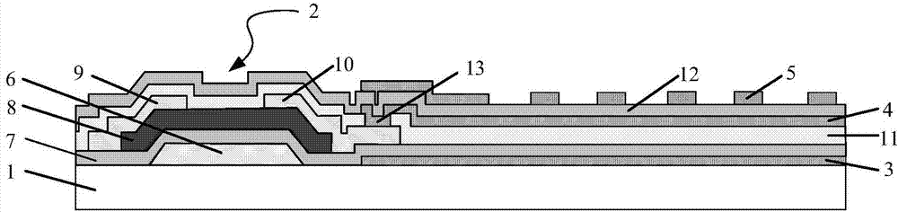
[0092] Figure 4 A schematic structural diagram of the array substrate provided in Embodiment 2 of the present invention, as shown in Figure 4 As shown, the array substrate is an FFS type array substrate, and the array substrate includes: a base substrate 1, a thin film transistor 2, a first common electrode 3, a pixel electrode 4 and a second common electrode 5, wherein the thin film transistor 2, the first A common electrode 3, pixel electrode 4 and second common electrode 5 are all formed above the base substrate 1, wherein the pixel electrode 4 is located between the first common electrode 3 and the second common electrode 5, and the pixel electrode 4 and the thin film transistor The drain 10 of 2 is electrically connected, the pixel electrode 4 is insulated from both the first common electrode 3 and the second common electrode 5 , and the potentials of the first common electrode 3 and the second common electrode 5 are equal.
[0093] The thin film transistor comprises: ...
PUM
 Abstract
Description
Claims
Application Information