Touch screen and manufacturing method of touch screen
A touch screen, non-transparent technology, applied in the input/output process of data processing, instruments, electrical digital data processing and other directions, can solve the problem of transparent key area affecting users' visual perception and other issues
- Summary
- Abstract
- Description
- Claims
- Application Information
AI Technical Summary
Problems solved by technology
Method used
Image
Examples
Embodiment 1
[0018] This embodiment provides a touch screen, which is suitable for various mobile terminals.
[0019] Such as Figure 2D Shown is a schematic structural diagram of the touch screen of this embodiment. The touch screen 200 includes a glass cover 201 , an ink layer 202 and a first non-transparent insulating layer 203 .
[0020] Wherein, the surface of the glass cover 201 is provided with a key area 204; the ink layer 202 is formed on the glass cover 201 and is located around the key area 204; the first non-transparent insulating layer 203 is formed on the glass cover 201 and is located in the key area 204 , that is, the ink layer 202 surrounds the first non-transparent insulating layer 203 .
[0021] In this embodiment, the first non-transparent insulating layer 203 and the ink layer 202 have different colors. The first non-transparent insulating layer 203 in this embodiment may specifically be a non-transparent insulating ink layer, and the specific material may be insula...
Embodiment 2
[0034] This embodiment makes further supplementary descriptions to Embodiment 1.
[0035] Such as Figure 3C As shown, in the touch screen 300 in this embodiment, in addition to the parts described in the first embodiment, a logo (Logo) area 301 is also provided on the glass cover 201 . On the sign area 301 , a second non-transparent insulating layer 302 formed simultaneously with the first non-transparent insulating layer is disposed on the sign area 301 , and the second non-transparent insulating layer 302 may specifically be a second non-transparent insulating ink layer. The second non-transparent insulating layer 302 and the first non-transparent insulating layer 203 are made of the same color and the same material
[0036] In this embodiment, the marking area 301 is a preset position on the glass cover 201 , and an ink layer 303 may be formed around the marking area 301 . The height of the second non-transparent insulating layer 302 is equal to the height of the ink lay...
Embodiment 4
[0047] This embodiment provides a method for manufacturing a touch screen, which is used to manufacture the touch screen of Embodiment 1.
[0048] Such as Figure 4 As shown, it is a schematic flow chart of the manufacturing method of the touch screen in this embodiment. The manufacturing method of the touch screen includes;
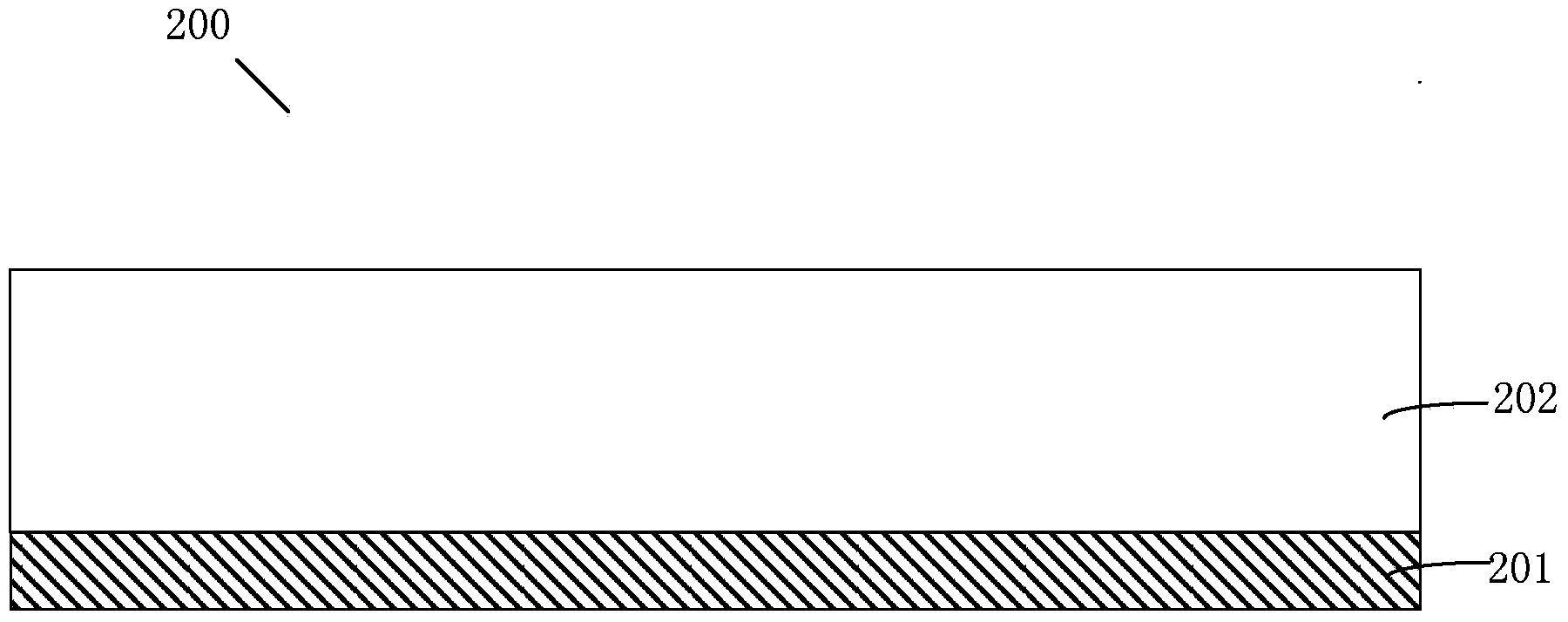
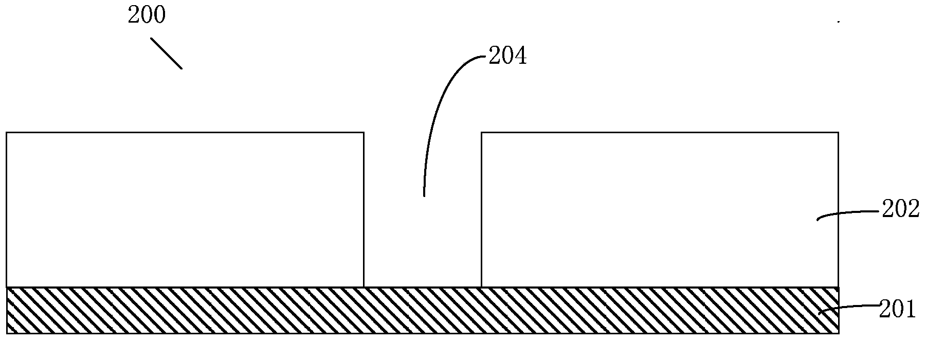
[0049] Step 401 , forming an ink layer around the key area of the glass cover.
[0050]The glass cover plate in this embodiment is transparent glass, and the ink layer can be formed by applying ink multiple times and curing it, and the hollowed out part of the ink layer is the keypad.
[0051] Step 402, forming a first non-transparent insulating layer on the keypad.
[0052] Specifically, the first non-transparent insulating layer may be a non-transparent insulating ink layer, and the non-transparent insulating ink layer may be realized by printing and curing. The upper surface of the first non-transparent insulating layer may be flush with the upp...
PUM
 Abstract
Description
Claims
Application Information


