Test circuit, display device and test method of driving circuit
A technology for testing circuits and driving circuits, used in static indicators, instruments, etc., can solve the problem of inability to determine the specific location of abnormal operation of the driving circuit, and achieve the effect of improving performance and yield
- Summary
- Abstract
- Description
- Claims
- Application Information
AI Technical Summary
Problems solved by technology
Method used
Image
Examples
Embodiment 1
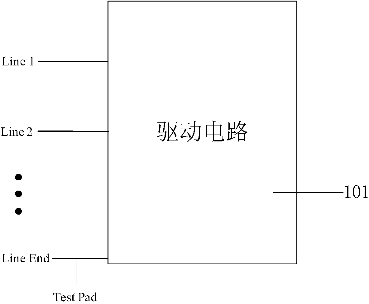
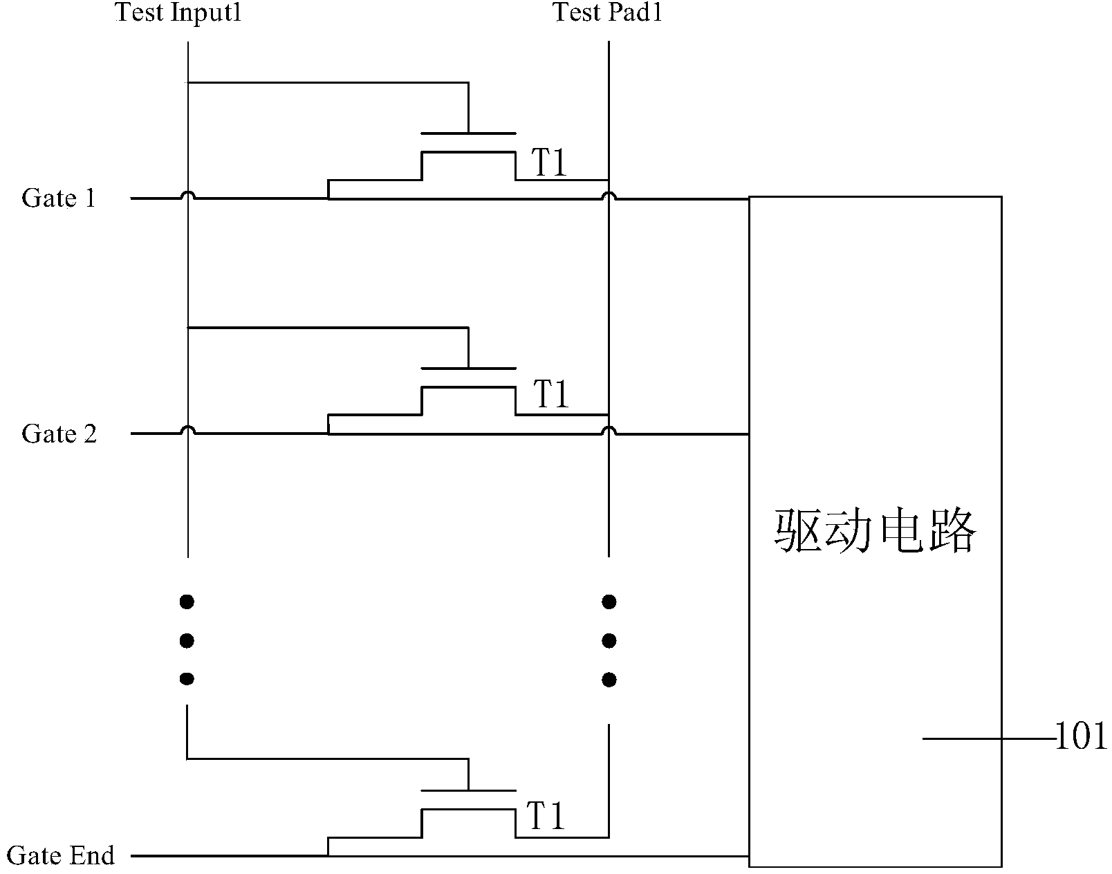
[0031] figure 2 It is a schematic structural diagram of a test circuit provided by Embodiment 1 of the present invention. Such as figure 2 As shown, the test circuit includes a first signal input line Test Input1, a first signal output line Test Pad1 and a plurality of first thin film transistors T1. The first signal input line Test Input1 is connected to the gate of the first thin film transistor T1, the first signal output line Test Pad1 is connected to the first electrode of the first thin film transistor T1, and the first thin film The second pole of the transistor T1 is connected to the driving circuit 101 through gate lines (Gate 1, Gate 2 . . . Gate End). Optionally, the driving circuit 101 includes a gate driving circuit, a reset driving circuit, and an emission driving circuit. In practical applications, the test circuit can also be applied to other driving circuits. The test circuit provided in this embodiment can not only evaluate the overall driving effect of...
Embodiment 2
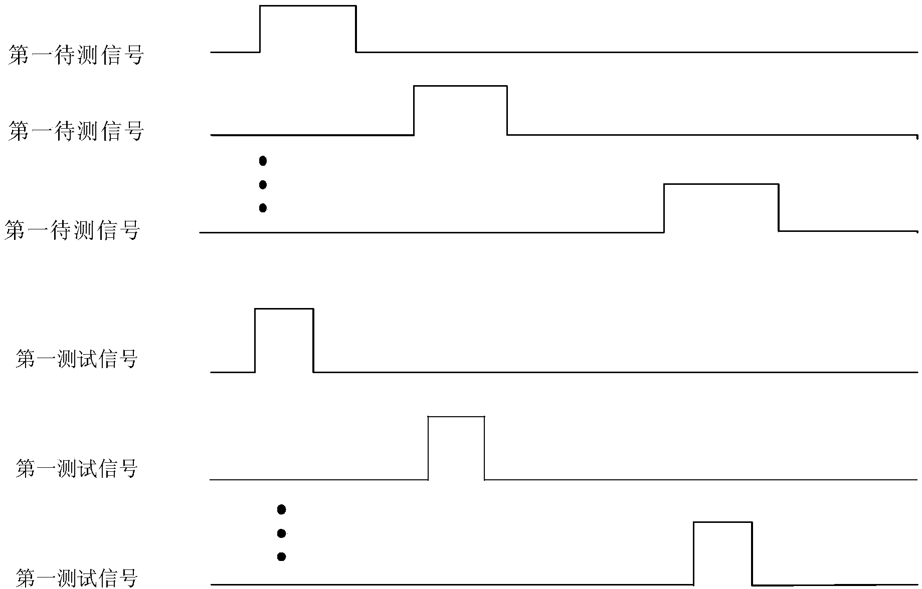
[0037] Figure 4 It is a schematic structural diagram of a test circuit provided by Embodiment 2 of the present invention. Such as Figure 4 As shown, the test circuit includes a first signal input line Test Input1, a first signal output line Test Pad1 and a plurality of first thin film transistors T1. The first signal input line Test Input1 is connected to the gate of the first thin film transistor T1, the first signal output line Test Pad1 is connected to the first electrode of the first thin film transistor T1, and the first thin film The second pole of the transistor T1 is connected to the driving circuit 101 through gate lines (Gate 1, Gate 2 . . . Gate End). Optionally, the drive circuit includes a gate drive circuit, a reset drive circuit, and an emission drive circuit. In practical applications, the test circuit can also be applied to other driving circuits. The test circuit provided in this embodiment can not only evaluate the overall driving effect of the driving...
Embodiment 3
[0044] Image 6 It is a schematic structural diagram of a test circuit provided by Embodiment 3 of the present invention. Such as Image 6 As shown, the test circuit includes a first signal input line Test Input1, a second signal input line Test Input2, a first signal output line Test Pad1, a second signal output line Test Pad2, a plurality of first thin film transistors T1 and a plurality of The second thin film transistor T2. The first signal input line Test Input1 is connected to the gate of the first thin film transistor T1, the first signal output line Test Pad1 is connected to the first electrode of the first thin film transistor T1, and the first thin film The second pole of the transistor T1 is connected to the driving circuit 101 through gate lines (Gate 1, Gate 2 . . . Gate End). The second signal input line Test Input2 is connected to the gate of the second TFT T2, the second signal output line Test Pad2 is connected to the first electrode of the second TFT T2, a...
PUM
 Abstract
Description
Claims
Application Information


