A test method for test circuit, display device and drive circuit

A technology for testing circuits and driving circuits, applied in static indicators, instruments, etc., can solve the problem of inability to determine the specific location of abnormal operation of the driving circuit, and achieve the effect of improving performance and yield

Active Publication Date: 2017-06-23
BOE TECH GRP CO LTD +1
View PDF5 Cites 0 Cited by
  • Summary
  • Abstract
  • Description
  • Claims
  • Application Information

AI Technical Summary

Problems solved by technology

[0005] In order to solve the above problems, the present invention provides a test circuit, a display device and a test method for a drive circuit, which is used to solve the problem that the test circuit in the prior art can only determine whether the drive circuit as a whole is working normally, but cannot determine whether the drive circuit is working abnormally. the specific location of the problem

Method used


Image

  • A test method for test circuit, display device and drive circuit
  • A test method for test circuit, display device and drive circuit
  • A test method for test circuit, display device and drive circuit

Examples


Embodiment 1

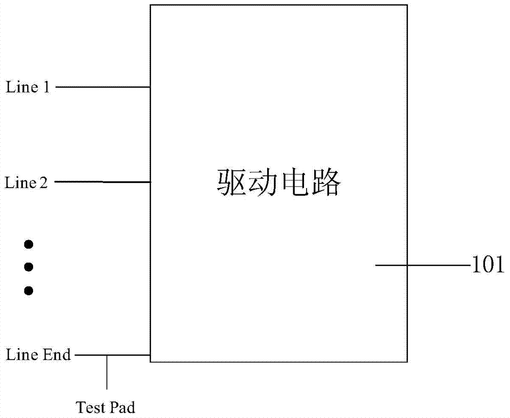
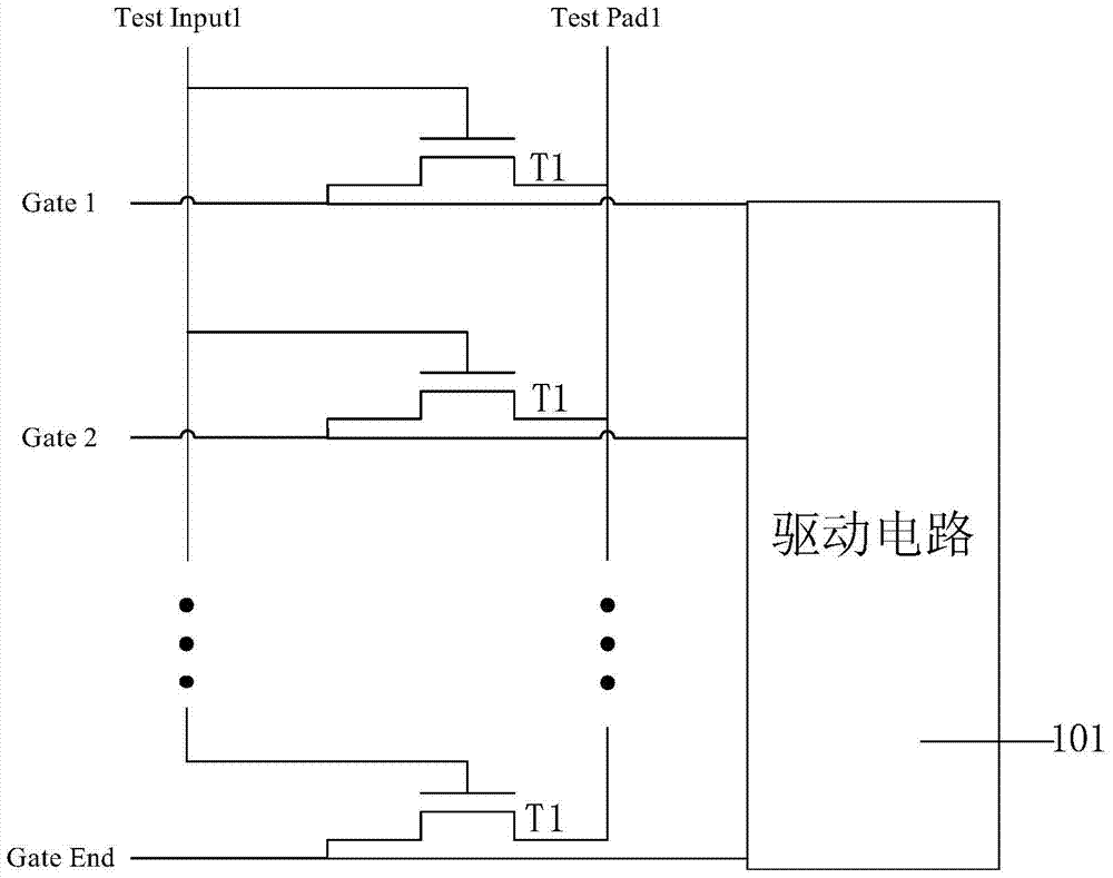
[0031] figure 2 It is a schematic structural diagram of a test circuit provided by Embodiment 1 of the present invention. Such as figure 2 As shown, the test circuit includes a first signal input line Test Input1, a first signal output line Test Pad1 and a plurality of first thin film transistors T1. The first signal input line Test Input1 is connected to the gate of the first thin film transistor T1, the first signal output line Test Pad1 is connected to the first electrode of the first thin film transistor T1, and the first thin film The second pole of the transistor T1 is connected to the driving circuit 101 through gate lines (Gate 1, Gate 2 . . . Gate End). Optionally, the driving circuit 101 includes a gate driving circuit, a reset driving circuit, and an emission driving circuit. In practical applications, the test circuit can also be applied to other driving circuits. The test circuit provided in this embodiment can not only evaluate the overall driving effect of...

Embodiment 2

[0037] Figure 4 It is a schematic structural diagram of a test circuit provided by Embodiment 2 of the present invention. Such as Figure 4 As shown, the test circuit includes a first signal input line Test Input1, a first signal output line Test Pad1 and a plurality of first thin film transistors T1. The first signal input line Test Input1 is connected to the gate of the first thin film transistor T1, the first signal output line Test Pad1 is connected to the first electrode of the first thin film transistor T1, and the first thin film The second pole of the transistor T1 is connected to the driving circuit 101 through gate lines (Gate 1, Gate 2 . . . Gate End). Optionally, the drive circuit includes a gate drive circuit, a reset drive circuit, and an emission drive circuit. In practical applications, the test circuit can also be applied to other driving circuits. The test circuit provided in this embodiment can not only evaluate the overall driving effect of the driving...

Embodiment 3

[0044] Image 6 It is a schematic structural diagram of a test circuit provided by Embodiment 3 of the present invention. Such as Image 6 As shown, the test circuit includes a first signal input line Test Input1, a second signal input line Test Input2, a first signal output line Test Pad1, a second signal output line Test Pad2, a plurality of first thin film transistors T1 and a plurality of The second thin film transistor T2. The first signal input line Test Input1 is connected to the gate of the first thin film transistor T1, the first signal output line Test Pad1 is connected to the first electrode of the first thin film transistor T1, and the first thin film The second pole of the transistor T1 is connected to the driving circuit 101 through gate lines (Gate 1, Gate 2 . . . Gate End). The second signal input line TestInput2 is connected to the gate of the second thin film transistor T2, the second signal output line Test Pad2 is connected to the first electrode of the ...


PUM


Abstract

The present invention provides a test circuit, a display device and a test method for a drive circuit. The test circuit includes a first signal input line, a first signal output line, and a plurality of first thin film transistors. The first signal input line is connected to the first signal input line. The gate of the first thin film transistor is connected, the first signal output line is connected to the first pole of the first thin film transistor, and the second pole of the first thin film transistor is connected to the driving circuit, so that the In the case of the production process, the performance of the drive circuit is evaluated during the production process, and the abnormal position can be accurately determined to improve the performance and yield of the product.

Description

technical field [0001] The invention relates to the field of display technology, in particular to a test circuit, a display device and a test method for a drive circuit. Background technique [0002] Gate Driver on Array (GOA) technology is a process technology that directly manufactures a driving circuit on an array substrate, thereby replacing a driving chip made of an external silicon chip. The technology can reduce the technological process, reduce the technological cost, and improve the integration degree of the liquid crystal display panel. [0003] The production process of the driving circuit is complicated, and any abnormality in the process may cause the product to be defective. Therefore, a test circuit that can timely and effectively judge whether the driving circuit is operating effectively is needed. [0004] figure 1 It is a structural schematic diagram of a test circuit in the prior art. Such as figure 1 As shown, the test circuit tests the drive circuit ...

Claims


Application Information

Patent Timeline
Patent Type & Authority Patents(China)
IPC IPC(8): G09G3/00
Inventor 刘祺张蕾
Owner BOE TECH GRP CO LTD
Why Eureka
Try Eureka