Substrate with transparent electrode, manufacturing method thereof, and touch panel

A technology of transparent electrodes and transparent electrode layers, which is applied in the direction of cable/conductor manufacturing, circuits, electrical components, etc., can solve problems such as no research, and achieve the effect of improving identification

Active Publication Date: 2017-03-01
KANEKA CORP
View PDF8 Cites 0 Cited by
  • Summary
  • Abstract
  • Description
  • Claims
  • Application Information

AI Technical Summary

Problems solved by technology

However, in Patent Documents 3 and 4, there is no research on pattern recognition when the transparent electrode layer is patterned.

Method used


Image

  • Substrate with transparent electrode, manufacturing method thereof, and touch panel
  • Substrate with transparent electrode, manufacturing method thereof, and touch panel
  • Substrate with transparent electrode, manufacturing method thereof, and touch panel

Examples


Embodiment 1

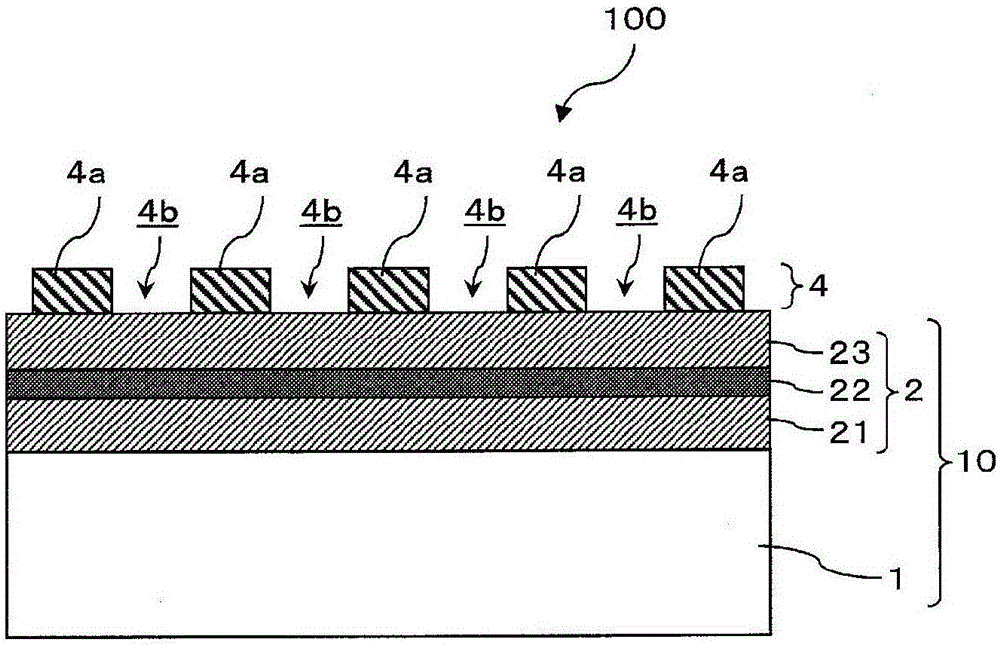
[0111] On one side of a biaxially stretched PET film with a thickness of 188 μm and a hard coat layer (refractive index 1.53) made of polyurethane resin formed on both sides, silicon Oxide (SiO x Layer) composed of medium refractive index transparent dielectric layer (first dielectric layer), high refractive index transparent dielectric layer (second dielectric layer) composed of niobium oxide, and silicon oxide (SiO 2 ) composed of a low refractive index dielectric layer (third dielectric layer).

[0112] First, using B-Si as the target material, while introducing oxygen / argon (20sccm / 400sccm) mixed gas into the device, the pressure in the device is 0.2Pa, the substrate temperature is -20°C, and the power density is 1.4W / cm 2 sputtering under conditions. Obtained SiO y The film thickness of the layer was 5 nm, and the refractive index was 1.65.

[0113] In the SiO x A high refractive index transparent dielectric layer is formed on the layer. Using niobium (Nb) as the ta...

Embodiment 2~9 and comparative example 1~3

[0119] Film thickness d of the second dielectric layer 2, The film thickness d of the third dielectric layer 3 And the film thickness of the transparent electrode layer was changed as shown in Table 1. Other than that, in the same manner as in Example 1, after forming the first dielectric layer, the second dielectric layer, the third dielectric layer, and the transparent electrode layer sequentially, patterning and heat treatment of the transparent electrode layer were performed.

Embodiment 10

[0122] The magnetic flux density at the time of forming the transparent electrode layer can be adjusted to 16 mT by changing the permanent magnet attached to the sputtering apparatus. The voltage of the MF power supply during sputtering film formation was 511V. Except for this, patterning and heat treatment of the transparent electrode layer were performed after sequentially forming the first dielectric layer, the second dielectric layer, the third dielectric layer, and the transparent electrode layer in the same manner as in Example 1 above.


PUM

PropertyMeasurementUnit
thicknessaaaaaaaaaa
thicknessaaaaaaaaaa
thicknessaaaaaaaaaa

Abstract

The object of the present invention is to provide a substrate with a transparent electrode and a manufacturing method thereof in which the pattern is not easily recognized visually when the transparent electrode layer is patterned. The substrate with a transparent electrode of the present invention has a first dielectric layer, a second dielectric layer, a third dielectric layer, and a patterned transparent electrode layer in order on at least one side of a transparent film. The first dielectric layer is a silicon oxide layer with SiOx as the main component, the second dielectric layer is a metal oxide layer with metal oxide as the main component, and the third dielectric layer is a silicon oxide layer with SiOy as the main component. . The transparent electrode layer is a conductive metal oxide layer mainly composed of indium-tin composite oxide. The refractive index n1 of the first dielectric layer, the refractive index n2 of the second dielectric layer, and the refractive index n3 of the third dielectric layer satisfy the relationship of n3<n1<n2. Each dielectric layer and transparent electrode layer preferably has a film thickness and a refractive index within a predetermined range.

Description

technical field [0001] The present invention relates to a substrate with a transparent electrode applicable to an electrostatic capacitive touch panel and a manufacturing method thereof. Moreover, this invention relates to the touch panel provided with the board|substrate with this transparent electrode. Background technique [0002] A substrate with a transparent electrode in which a transparent electrode layer is formed on a transparent substrate such as a film or glass can be used as a transparent electrode for displays such as touch panels, light-emitting elements, and photoelectric conversion elements. When the substrate with transparent electrodes is used for position detection of capacitive touch panels, the transparent electrode layer can be finely patterned. As a patterning method, for example, after forming a transparent electrode layer on substantially the entire surface of a transparent substrate, a method of removing the transparent electrode layer by etching o...

Claims


Application Information

Patent Timeline
Patent Type & Authority Patents(China)
IPC IPC(8): H01B5/14B32B9/00C23C14/08C23C14/10C23C14/34H01B13/00
CPCC23C14/0036C23C14/083C23C14/086C23C14/10C23C14/34C23C14/35C23C14/562G06F3/0412G06F2203/04103G06F3/0443C23C14/08G06F1/16G06F2203/04112G06F3/0448
Inventor 上田拓明近藤晃三檀野和久
Owner KANEKA CORP
Why Eureka
Try Eureka