
High-performance anti-interference drive circuit suitable for IGBT and MOS

A drive circuit, high-performance technology, applied in the direction of logic circuits using optoelectronic equipment, logic circuits using specific components, electrical components, etc., can solve problems such as large PCB volume, high component costs, and complex circuit structures, and achieve element The effect of using less components, high operational stability, and simple circuit structure

Inactive Publication Date: 2015-01-28
HANGZHOU SONNY ENERGY TECH CO LTD
View PDF2 Cites 1 Cited by
  • Summary
  • Abstract
  • Description
  • Claims
  • Application Information

AI Technical Summary

Problems solved by technology

However, during the working process of the general drive circuit, it is required to accurately control the on and off of the MOS or IGBT according to the PWM signal sent by the DSP, so as to realize the functions required by the photovoltaic inverter; but due to the high and low frequency signals inside the inverter In the case of overlapping or unreasonable layout, some other signals will interfere with the PWM signal sent by the DSP, resulting in the inability to correctly control the turn-on and turn-off of the MOS or IGBT, resulting in damage to the MOS or IGBT
However, although some existing anti-interference drive circuits can achieve anti-interference effect, the circuit structure is complex, the cost of components used is high, and the required PCB volume is relatively large.

Method used


Image

  • High-performance anti-interference drive circuit suitable for IGBT and MOS

Examples


Embodiment Construction

[0012] The present invention will be further described below in conjunction with the accompanying drawings and embodiments, but not as a basis for limiting the present invention.

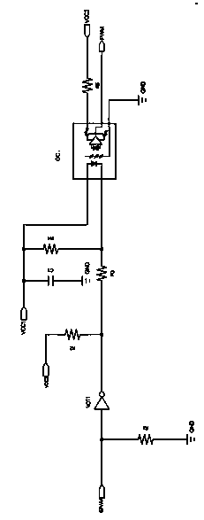
[0013] Example. A high-performance anti-interference driving circuit suitable for IGBT and MOS, such as figure 1 Shown: includes an optocoupler OC and a NOT gate circuit NOT1 whose input terminal is connected to the IO port or PWM port of the DSP; the anode of the light-emitting diode in the optocoupler OC is connected to the first power supply VCC1, and the light-emitting diode in the optocoupler OC The cathode is connected to the output terminal of the NOT gate circuit NOT1 through the first current limiting resistor R3, the output terminal of the NOT gate circuit NOT1 is also provided with a pull-up resistor R2, and the pull-up resistor R2 is connected to the second power supply VCC2, the The signal output end of the optocoupler OC is connected to the controlled IGBT or MOS. A voltage stabilizi...


PUM


Abstract

The invention discloses a high-performance anti-interference drive circuit suitable for an IGBT and an MOS. The high-performance anti-interference drive circuit suitable for the IGBT and the MOS comprises an optocoupler (OC) and a not-gate circuit (NOT1), wherein the input end of the not-gate circuit (NOT1) is connected to an IO port or a PWM port of a DSP. An anode of an LED inside the optocoupler (OC) is connected to a first power source (VCC1), a cathode of the LED inside the optocoupler (OC) is connected to the output end of the not-gate circuit (NOT1) through a first current-limiting resistor (R3), the output end of the not-gate circuit (NOT1) is further provided with a pull-up resistor (R2), the pull-up resistor (R2) is connected with a second power source (VCC2), and the signal output end of the optocoupler (OC) is connected to the controlled IGBT or the controlled MOS. The high-performance anti-interference drive circuit suitable for the IGBT and the MOS can play a role of efficient EMI resistance, so that the purpose of preventing the MOS or the IGBT from being switched on and switched off accidentally can be achieved, in addition, the circuit structure is simple, the cost is low, and the needed size is small.

Description

technical field [0001] The invention relates to an anti-jamming circuit, in particular to a high-performance anti-jamming driving circuit suitable for IGBT and MOS used in photovoltaic inverters. Background technique [0002] A photovoltaic inverter usually includes a drive circuit for controlling the turn-on and turn-off of MOS or IGBT. However, during the working process of the general drive circuit, it is required to accurately control the on and off of the MOS or IGBT according to the PWM signal sent by the DSP, so as to realize the functions required by the photovoltaic inverter; but due to the high and low frequency signals inside the inverter In the case of overlapping or unreasonable layout, some other signals will interfere with the PWM signal sent by the DSP, resulting in the inability to correctly control the turn-on and turn-off of the MOS or IGBT, resulting in damage to the MOS or IGBT. However, although some existing anti-jamming driving circuits can achieve t...

Claims


Application Information

Patent Timeline
Patent Type & Authority Applications(China)
IPC IPC(8): H03K17/567H03K19/14
Inventor 李新富欧余斯程亮亮
Owner HANGZHOU SONNY ENERGY TECH CO LTD
Learn More