An Efficient Substrate Lift-Off Method
A substrate, high-efficiency technology, applied in electrical components, semiconductor/solid-state device manufacturing, circuits, etc., can solve problems such as easy damage of epitaxial structures
- Summary
- Abstract
- Description
- Claims
- Application Information
AI Technical Summary
Problems solved by technology
Method used
Image
Examples
Embodiment Construction
[0040] The present invention will be described in detail below in conjunction with the accompanying drawings and specific embodiments.
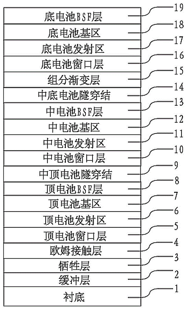
[0041] like figure 1 As shown, the present invention discloses a solar cell epitaxial structure with a substrate that can be peeled off. On the surface of the substrate 1 from bottom to top, epitaxial buffer layer 2, sacrificial layer 3, ohmic contact layer 4, top cell window layer 5, Top cell emission region 6, top cell base region 7, top cell BSF layer 8, middle top cell tunnel junction 9, middle cell window layer 10, middle cell emission region 11, middle cell base region 12, middle cell BSF layer 13, Middle bottom cell tunnel junction 14 , composition graded layer 15 , bottom cell window layer 16 , bottom cell emitter region 17 , bottom cell base region 18 and bottom cell BSF layer 19 .
[0042] The substrate 1 is a 4-inch GaAs substrate with a thickness of 400 μm. The material of the buffer layer 2 is GaAs III-V compound with a thickne...
PUM
 Abstract
Description
Claims
Application Information

