Method for manufacturing antenna part

A technology for antenna elements and manufacturing methods, applied in antennas, semiconductor/solid-state device manufacturing, electrical components, etc., can solve the problems of increased manufacturing hours, higher manufacturing costs, and more parts, and achieve improved price advantages and productivity Improved effect

Inactive Publication Date: 2015-02-11
SUMIDA CORP
View PDF7 Cites 3 Cited by
  • Summary
  • Abstract
  • Description
  • Claims
  • Application Information

AI Technical Summary

Problems solved by technology

Therefore, the number of parts increases, which increases the manufacturing cost for assembly and increases the number of manufacturing man-hours.

Method used


Image

  • Method for manufacturing antenna part
  • Method for manufacturing antenna part
  • Method for manufacturing antenna part

Examples


Embodiment Construction

[0024] Hereinafter, an embodiment for implementing the present invention (hereinafter, referred to as an "embodiment") will be described in detail with reference to the accompanying drawings.

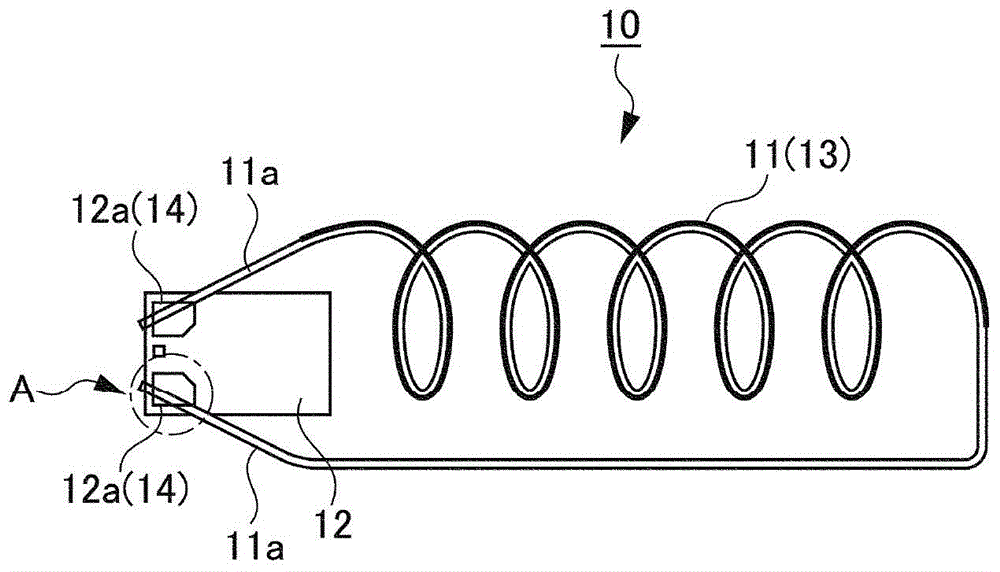
[0025] figure 1 Shown is a schematic diagram of an example of an antenna element manufactured by applying the manufacturing method according to the present invention. In this figure, the antenna element 10 includes a coil member 11 and a semiconductor substrate 12 .

[0026] The coil component 11 is a coil-shaped antenna coil formed by winding a wire 13 with a predetermined number of turns, and connecting ends 11 a and 11 a are led out at both ends thereof as connecting portions for connecting with the semiconductor substrate 12 , respectively. connect.

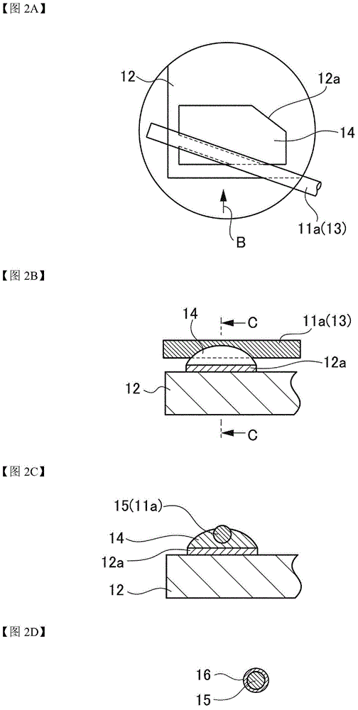
[0027] The semiconductor substrate 12 is an IC chip, and a part of the upper surface thereof is provided with conductive terminals, ie, pads 12a and 12a, which are connection regions, and the conductive terminals are formed of condu...


PUM

PropertyMeasurementUnit
diameteraaaaaaaaaa
thicknessaaaaaaaaaa
thicknessaaaaaaaaaa

Abstract

Provided is a method of manufacturing an antenna part that can be produced easily and inexpensively, the method comprising the steps of: forming a coil part 11 by a wire material 13 having an insulation coating 16, and removing the insulation coating 16 from both end portions 11a of the coil part 11; forming a connection region 12a of an electrically-conductive metal on the semiconductor substrate 12, and further forming a solder layer 14 on the connection region 12a; wiring the coil part 11 on the connection region 12a so that each end portion 11a of the coil part 11 to be in contact with the solder layer 14; and melting the solder layer 14 by heat to allow each end portions 11a to enter into the solder layer 14, and thus to electrically connect the connection region 12a and the coil part 11 through the solder layer 14.

Description

technical field [0001] The present invention relates to a method of manufacturing an antenna element, and more particularly, to a method of manufacturing an antenna element for electrically connecting and fixing a connecting portion of a wire rod drawn from a coil component for antenna to a semiconductor substrate. Background technique [0002] In general, as an antenna element in which an IC chip and a winding coil are integrated, such as an IC card for entering or leaving a station, or a transmitting antenna for a remote control key of a car or a house, etc., it is known that the IC chip and the IC chip are connected with a bonding wire by a bonding wire. Connections made by winding coils. [0003] Patent Document 1 describes a method of forming a sphere by applying arc discharge to the tip of a conductive wire having an insulating coating on the outside, and then ultrasonically vibrating the sphere to connect the sphere to a pad of a semiconductor substrate. [0004] How...

Claims


Application Information

Patent Timeline
Patent Type & Authority Applications(China)
IPC IPC(8): H01Q1/12H01L21/60
CPCH01Q7/00G06K19/07754G06K19/07779H01L24/05H01L24/48H01L2224/4813H01L2224/05012H01L24/85H01L2224/85801H01L2224/45144H01L2224/45147H01L2224/45015H01L2924/00014H01L2924/12042H01L2224/85205H01L24/45H01L2224/48092Y10T29/49018H01L2924/20753H01L2924/20754H01L2924/20756H01L2924/20755H01L2224/05599H01L2924/00
Inventor 森本泰德畑山佳之
Owner SUMIDA CORP
Why Eureka
Try Eureka