

Semiconductor device
A semiconductor and signal technology, applied in signal transmission systems, instruments, analog-to-digital converters, etc., can solve the problems of large clock signal cycle, peripheral circuits cannot follow the internal clock, and cannot perform comparison operations, etc., to achieve the effect of accurate cycle
- Summary
- Abstract
- Description
- Claims
- Application Information
AI Technical Summary
Problems solved by technology
Method used
Image

Examples
no. 1 example
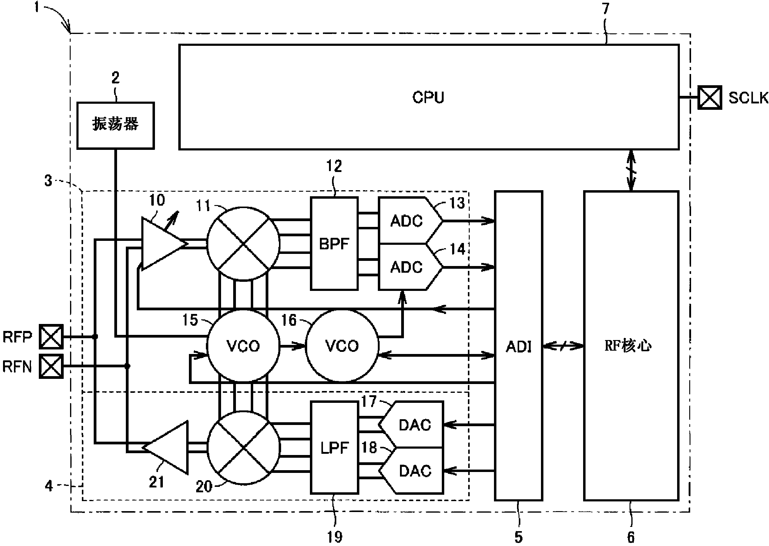
[0040] Such as figure 1 As shown, the wireless communication semiconductor device 1 according to the first embodiment of the present application includes an oscillator 2, a receiving system analog circuit 3, a transmission system analog circuit 4, an A / D interface circuit (ADI) 5, an RF (radio frequency) core 6 and CPU (Central Processing Unit) 7 . The oscillator 2 generates an oscillation signal having a predetermined frequency, and supplies the oscillation signal to the receiving system analog circuit 3 .
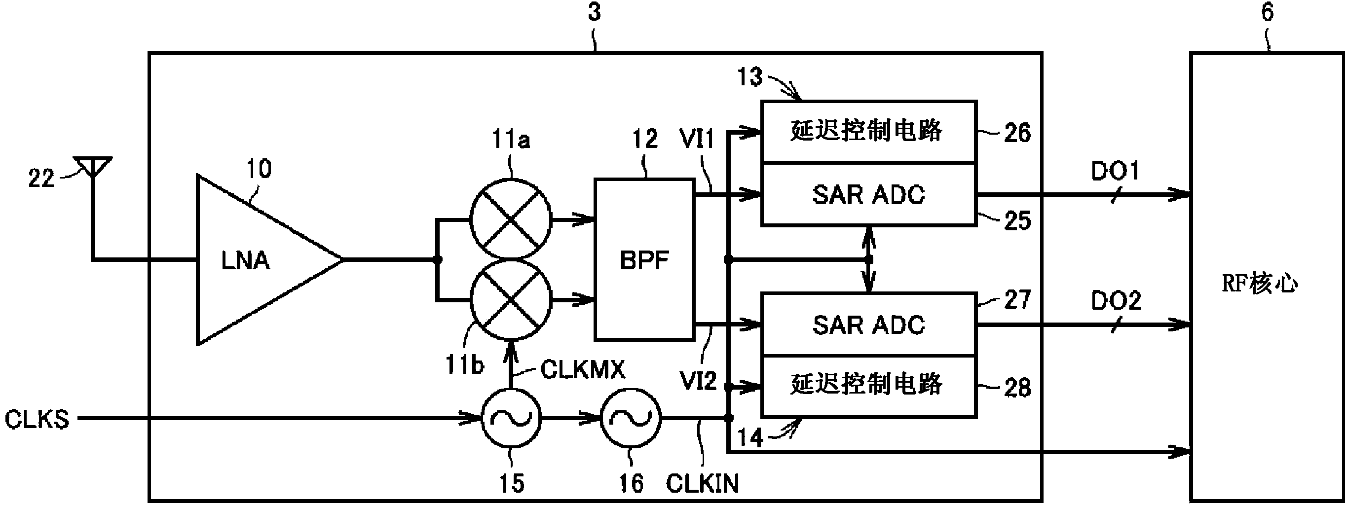
[0041] The reception system analog circuit 3 includes an LNA (Low Noise Amplifier) 10, a mixer 11, a BPF (Band Pass Filter) 12, ADCs (Analog to Digital Converters) 13 and 14, and a VCO (Voltage Controlled Oscillator) 15 and 16. The transmission system analog circuit 4 includes DACs (Digital to Analog Converters) 17 and 18 , an LPF (Low Pass Filter) 19 , a mixer 20 and a power amplifier 21 .
[0042] VCO 15 generates a local oscillation signal based on the oscillatio...
no. 2 example
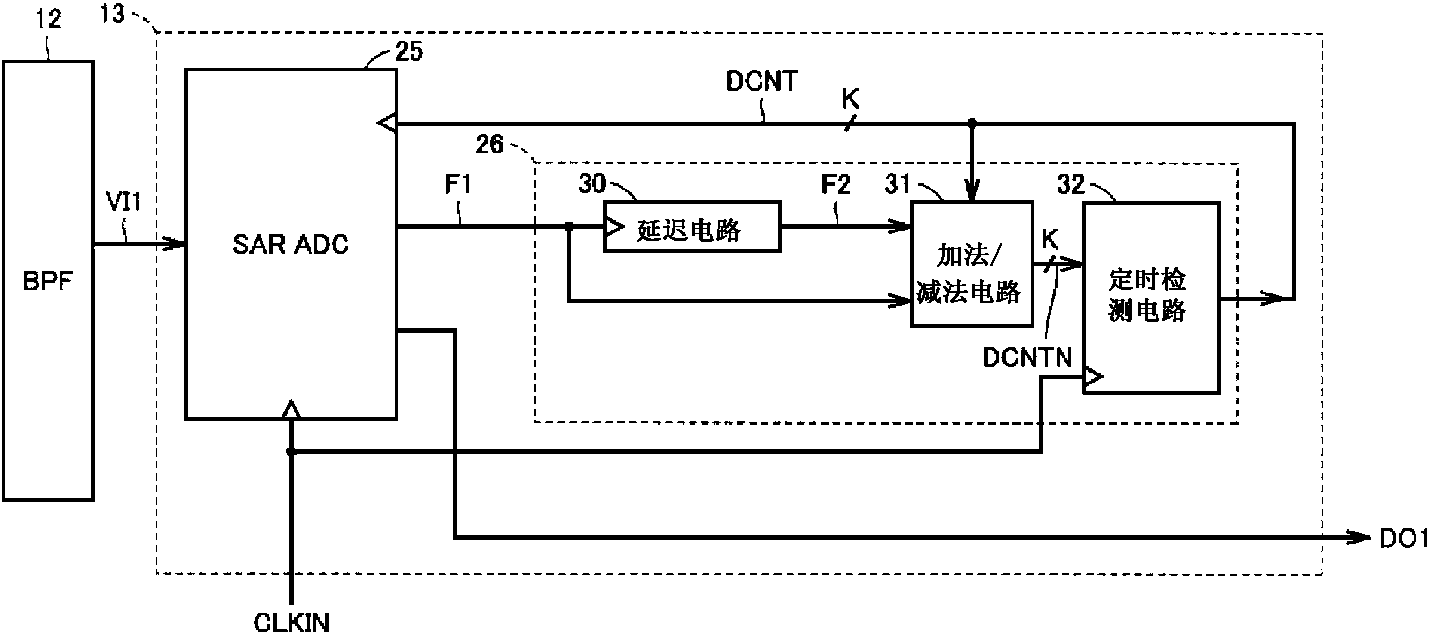
[0136] Figure 16 is a circuit block diagram showing the configuration of the ADC according to the second embodiment of the present application, and is to be used with image 3 Schematic for comparison. exist Figure 16 In this ADC, the addition / subtraction circuit 31 is composed of a combinational logic circuit 85 , and the timing detection circuit 32 is composed of a flip-flop 90 . The combinational logic circuit 85 includes inverters 86 and 87 , an AND gate 88 and an OR gate 89 .
[0137] The delay control signal DCNT is a one-bit signal, and is supplied to the asynchronous successive approximation ADC 25 and one input node of the AND gate 88 . The output signal F2 of the delay circuit 30 is inverted by the inverter 86 and supplied to the other input node of the AND gate 88 . An output signal of the AND gate 88 is supplied to one input node of the OR gate 89 . The signal F1 is inverted by the inverter 87 and supplied to the other input node of the OR gate 89 . The out...
no. 3 example
[0144] Figure 17is a circuit block diagram showing the configuration of the ADC according to the third embodiment of the present application, and is to be used with image 3 Schematic for comparison. exist Figure 17 , the ADC with image 3 The ADC 13 is different in that the addition / subtraction circuit 31 and the timing detection circuit 32 are replaced by an addition / subtraction circuit 91 and a timing detection circuit 92, respectively. The bit width of the delay control signal DCNT is 4 bits.
[0145] The addition / subtraction circuit 91 generates the delay control signal DCNTN used in the next comparison period based on the delay control signal DCNT determined in the previous comparison period, and the logic levels of the signals F1 and F2. Here, each of the delay control signals DCNT and DCNTN is a thermometer code.
[0146] The thermometer code is a code expressed in a bit sequence of binary notation, and it changes sequentially from 0 to 1 from the smallest bit e...
PUM
 Abstract
Description
Claims
Application Information