Method for producing alloy phase change material nano-dot matrix

A kind of alloy phase and nanotechnology, applied in the direction of metal material coating technology, nanotechnology, nanotechnology, etc., can solve the problems of high production cost and complicated preparation process, achieve high uniformity, simple process, reduce voltage and power consumption Effect

Inactive Publication Date: 2009-12-16
NANJING UNIV
View PDF6 Cites 0 Cited by
  • Summary
  • Abstract
  • Description
  • Claims
  • Application Information

AI Technical Summary

Problems solved by technology

[0003] According to the applicant's knowledge, electron beam exposure or nanoimprinting is mostly used to prepare small-sized C-RAM chalcogenide nano-arrays, and the preparation process is complicated and the production cost is high.

Method used


Image

  • Method for producing alloy phase change material nano-dot matrix

Examples


Embodiment 1

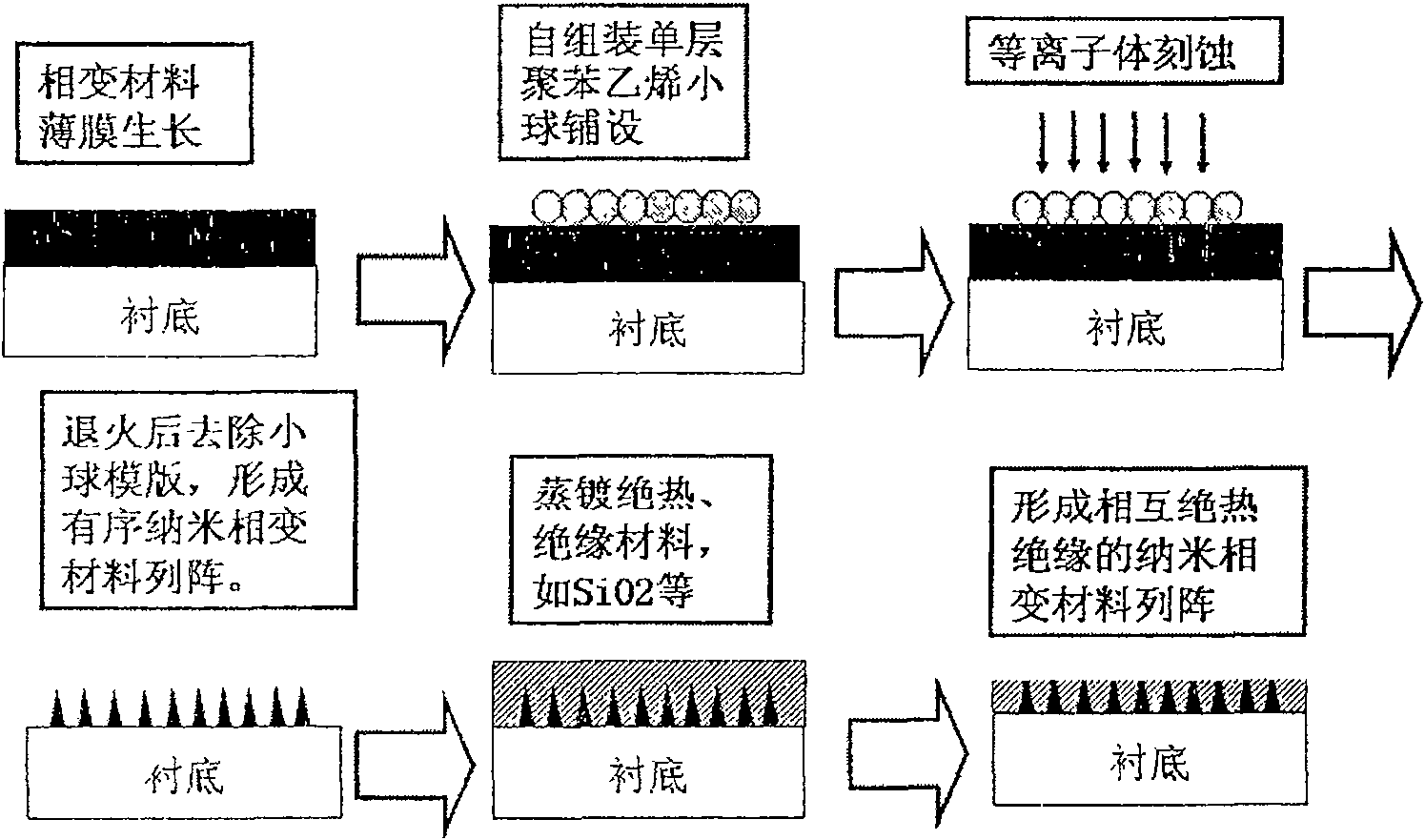
[0022] A method for preparing an alloy phase change material nano-lattice in this embodiment is shown in FIG. 1, and the preparation process includes the following steps:

[0023] The first step is to lay a single layer of nano-polystyrene beads PS beads on the water surface: use the surface tension of the water to lay a single layer of PS colloid (50nm-500nm) beads on the water surface to form a high density on the water surface , Large area, orderly arranged single-layer PS colloidal sphere membrane, let the PS colloid sphere membrane stand on the water surface for about 10 minutes.

[0024] The second step is to fish the single-layer film of the PS ball: use the substrate sheet covered with the silicon antimony tellurium film to pick up the PS ball film, and evaporate and dry naturally in the air; in order to make the PS colloidal ball film better adhere to the substrate Together, the dried products are annealed at 60±5°C for 1±0.1 hours.

[0025] The third step, reactive ion e...

Embodiment 2

[0030] The basic steps of the method for preparing the alloy phase change material nano-lattice in this embodiment are the same as those in the first embodiment, but the difference lies in:

[0031] 1. In the second step, a substrate sheet covered with germanium, antimony, tellurium film is used to pick up the PS ball film, and then it is naturally volatilized and dried in the air and annealed.

[0032] 2. In the third step, a single-layer polystyrene ball attached to the germanium, antimony, tellurium film is used as a mask, and carbon tetrafluoride gas is used to perform reactive ion etching on the sample (ME3A type multifunctional reactive ion Etching machine) to form a germanium-antimony-tellurium nano-array.

[0033] 3. In the fourth step, put the products of the previous step into acetone ultrasonic solution to soak, and completely remove the polystyrene beads.

[0034] 4. In the fifth step, the zirconium dioxide thermal insulation and insulating material is evaporated on th...


PUM


Abstract

The invention relates to a preparing method of nanometer dot matrix for alloy phase change material, belonging to nanometer electronic and nanometer photoelectric device material technical field. The preparing method is characterized in that monolayer nanometer polystyrene globule-PS globule is laid on water surface; backing material is used to catch the monolayer membrane of the PS globule; reaction ion is used to etch; PS mask is eliminated by annealing; heat insulating material is evaporated and plated on the upper layer of nanometer array; each step of evaporation plating layer is eliminated; then mutually insulated nanometer phase change material array is formed. The nanometer dot matrix method for preparing alloy phase change material, compatible with current micro electric craft has the advantages of obtaining germanium-antimony-tellurium and silicon-antimony-tellurium dot matrix with high density and uniformity without using high cost superfine process technique, enable the size of the active area of phase-change material to reach tens of nanometers or even several nanometers, being helpful to greatly decrease the voltage and power consumption needed by the phase change of material, and enable chalcogenide compound nanometer phase change material to walk out of the laboratories for the industrialized production.

Description

Technical field [0001] The invention relates to a method for preparing an alloy phase change material nano lattice, in particular to a method for preparing a size-controllable germanium antimony tellurium (GexSbyTez) and silicon antimony tellurium (SixSbyTez) alloy phase change material nano lattice, which belongs to nanometer Electronic and nano-optoelectronic device materials technology field. Background technique [0002] Chalcogenide germanium antimony tellurium (GexSbyTez) or silicon antimony tellurium (SixSbyTez) phase change semiconductor memory (PCRAM for short) is a new type of semiconductor memory, which is non-volatile compared with a variety of existing semiconductor storage technologies. , Long cycle life, low power consumption, multi-level storage, high-speed reading, anti-interference and other advantages. However, in order to make PCRAM devices show superiority and competitiveness compared with commercialized memory, they must be made into nanoelectronic devices, ...

Claims


Application Information

Patent Timeline
Patent Type & Authority Patents(China)
IPC IPC(8): B82B3/00C23F1/12C23C14/22
Inventor 徐岭戴明甘新慧徐骏马忠元李卫李伟赵伟明孙萍陈坤基
Owner NANJING UNIV
Why Eureka
Try Eureka