Method for fabricating semiconductor layer having textured surface and method for fabricating solar cell

A solar cell and textured surface technology, which is applied in semiconductor/solid-state device manufacturing, semiconductor devices, circuits, etc., can solve problems such as inability to provide thin chips, mass production, and difficulty in large-scale production

Active Publication Date: 2013-08-21
IND TECH RES INST
View PDF12 Cites 0 Cited by
  • Summary
  • Abstract
  • Description
  • Claims
  • Application Information

AI Technical Summary

Problems solved by technology

[0005] However, the thin chips produced by the above method have poor flatness, are not easy to be large-scale, and cannot be mass-produced.
In addition, current fabrication methods do not provide thin chips with textured surface structures

Method used


Image

  • Method for fabricating semiconductor layer having textured surface and method for fabricating solar cell
  • Method for fabricating semiconductor layer having textured surface and method for fabricating solar cell
  • Method for fabricating semiconductor layer having textured surface and method for fabricating solar cell

Examples


Embodiment 1

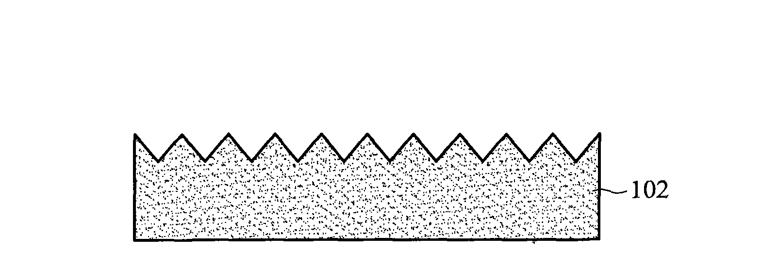
[0067] First provide a patterned sapphire substrate, image 3 A scanning electron microscope image showing regular patterns on a sapphire substrate.

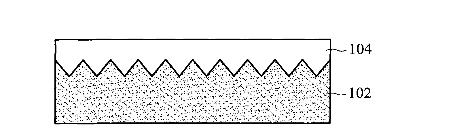
[0068] After that, silane (SiH 4 ) as a reaction gas, under the conditions of a coating temperature of about 200° C., a coating pressure of about 0.5 torr, and a coating power of about 200 W, microcrystalline silicon with a thickness of about 3 μm is formed on the patterned sapphire substrate.

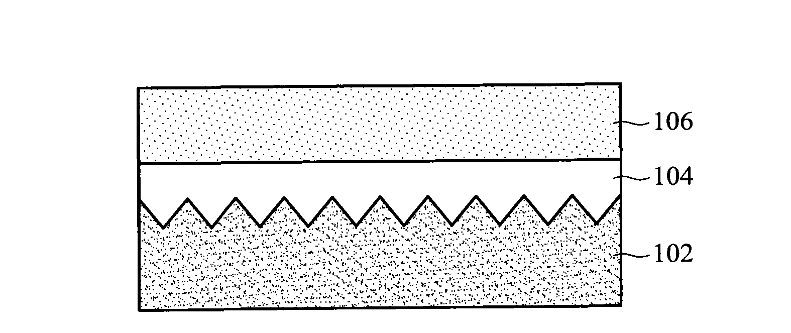
[0069] Next, a conductive silver paste (DuPont PV-159) was coated on the surface of the microcrystalline silicon. Afterwards, the patterned sapphire substrate is placed in an oven at 600°C for 30 minutes of heat treatment, and the microcrystalline silicon layer can be transferred to the conductive silver glue to obtain a thin silicon layer with a regular pattern on the conductive silver glue. Figure 4 A scanning electron microscope image showing the textured surface structure of a thin silicon layer.

Embodiment 2

[0071] The preparation method of embodiment 2 is similar to embodiment 1, and the only difference is that conductive silver glue (DuPont PV-412) is coated on the microcrystalline silicon surface. Afterwards, the patterned sapphire substrate was placed in an oven at 250°C for 10 minutes of heat treatment, and then the microcrystalline silicon layer was transferred onto the conductive silver paste to obtain a thin silicon layer with a regular pattern on the conductive silver paste.

Embodiment 3

[0072] Embodiment 3 is made into a solar cell

[0073] Taking the thin silicon layer of Example 1, a silicon nitride anti-reflection layer was formed on the thin silicon layer by coating method. Afterwards, a silver metal layer is formed by electroplating to complete a thin solar cell, wherein the conductive silver paste can be used as a back contact, and the silver metal layer can be used as a front contact.


PUM

PropertyMeasurementUnit
thicknessaaaaaaaaaa
thicknessaaaaaaaaaa
thicknessaaaaaaaaaa

Abstract

The disclosure provides a method for fabricating a semiconductor layer having a textured surface, including: (a) providing a textured substrate; (b) forming at least one semiconductor layer on the textured substrate; (c) forming a metal layer on the semiconductor layer; and (d) conducting a thermal process to the textured substrate, the semiconductor layer and the metal layer, wherein the semiconductor layer is separated from the textured substrate by the thermal process to obtain the semiconductor layer having the metal layer and a textured surface.

Description

technical field [0001] The present invention relates to a method of making thin semiconductor layers, and in particular to a method of making semiconductor layers with textured surfaces. Background technique [0002] In order to reduce the production cost of solar cells, the technology of thin chips has been developed. The current method of making thin chips is to cut the chips thinner, but the chip is easy to break during the cutting process, and if it is subsequently assembled into a battery, it is also a challenge not to damage the thin chip during the assembly process. [0003] U.S. Patent No. 7,077,901 discloses a method for manufacturing a single crystal silicon wafer (single crystal silicon wafer), which first makes a porous layer (porous) on a single crystal silicon substrate, and then places the single crystal silicon substrate in a silicon solution. To form a single crystal layer on the porous layer. Afterwards, the porous layer is destroyed by external force to ...

Claims


Application Information

Patent Timeline
Patent Type & Authority Applications(China)
IPC IPC(8): H01L21/02H01L31/18
CPCH01L31/02363H01L31/1896Y02E10/50
Inventor 王珽玉陈建勋杜政勋贡中元
Owner IND TECH RES INST
Why Eureka
Try Eureka