

Method for preparing silver nanowire transparent electrode in large area and silver nanowire transparent electrode
A technology of silver nanowires and transparent electrodes, which is applied in the field of optoelectronics, can solve the problems such as the inability to realize the preparation of large-area silver nanowire transparent electrodes, achieve excellent conductivity and transmittance, expand the application range, and have high repeatability and reliability Effect
- Summary
- Abstract
- Description
- Claims
- Application Information
AI Technical Summary
Problems solved by technology
Method used
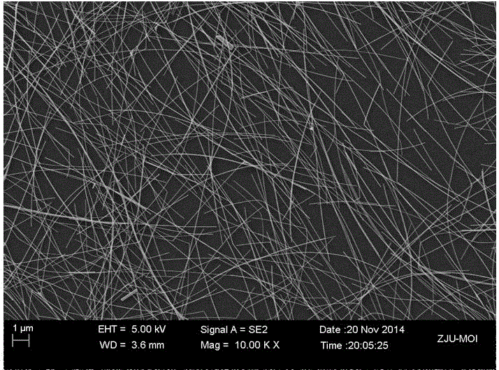
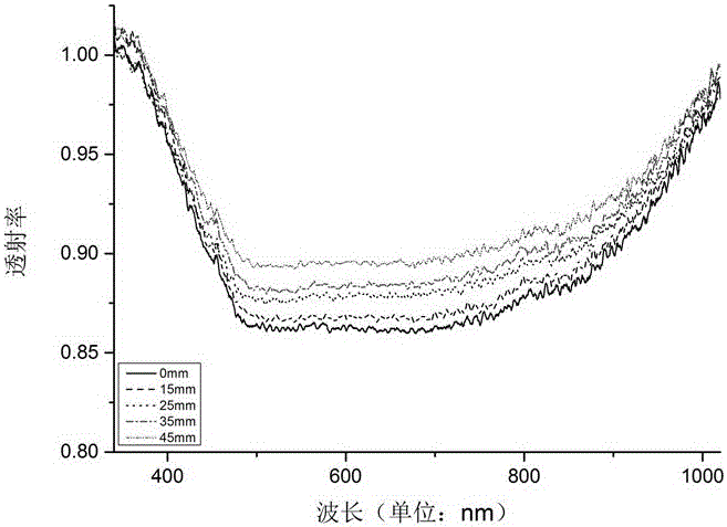
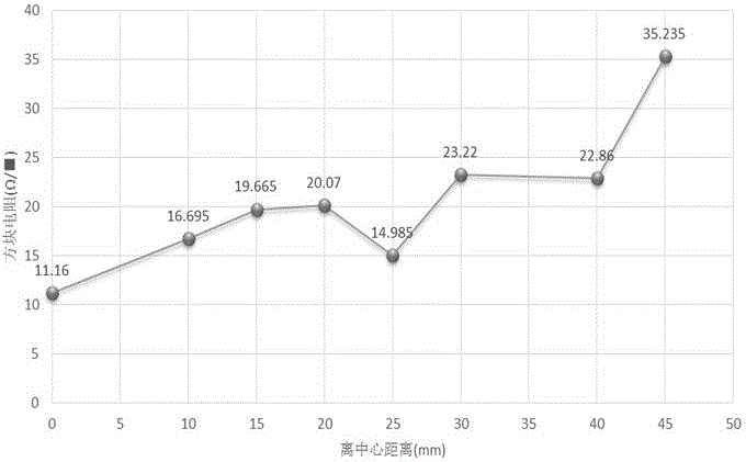
Image

Examples
Embodiment 1
[0031] The preparation method of the silver nanowire transparent electrode of the present embodiment comprises the following steps:
[0032] (1) Preparation of silver nanowire-photoresist suspension
[0033] Take an appropriate amount of silver nanowire solution, and use a centrifuge to separate the silver nanowire and solvent. After removing the solvent, mix the bottom silver nanowire with a positive photoresist (such as polymethyl acrylate PMMA, an electron beam sensitive positive photoresist). In the photoresist), shake until the silver nanowires are evenly dispersed in it to form a silver nanowire-photoresist suspension, where the concentration of the silver nanowires is about 5 mg / mL;
[0034] (2) Prepare the transparent substrate
[0035] Choose quartz glass with a diameter of 4'' as the transparent substrate, ultrasonically clean it with acetone, methanol, and isopropanol at room temperature for 5 minutes, soak in the mixed solution of ammonia water and hydrogen peroxi...
Embodiment 2
[0042] The preparation method of the silver nanowire transparent electrode of the present embodiment comprises the following steps:
[0043] (1) Preparation of silver nanowire-photoresist suspension
[0044] Take an appropriate amount of silver nanowire solution, and use a centrifuge to separate the silver nanowire and solvent. After removing the solvent, mix the bottom silver nanowire into negative photoresist (such as SU-8 series photoresist), and shake until the silver nanowire The wires are evenly dispersed in it to form a silver nanowire-photoresist suspension;
[0045] (2) Prepare the transparent substrate
[0046]Choose quartz glass with a diameter of 4'' as the transparent substrate, ultrasonically clean with acetone, methanol, and isopropanol at room temperature for 5 minutes, soak in ammonia water and hydrogen peroxide mixed solution at room temperature for 10 minutes, soak in piranha solution at room temperature for 20 minutes, and blow dry with dry nitrogen. Dry ...
PUM
| Property | Measurement | Unit |
|---|---|---|
| thickness | aaaaa | aaaaa |
| concentration | aaaaa | aaaaa |
Abstract
Description
Claims
Application Information