

Pixel structure and manufacturing method of cmos image sensor
An image sensor, pixel structure technology, applied in semiconductor/solid-state device manufacturing, electrical components, radiation control devices, etc., can solve the problems of power consumption process, depletion layer width, small thickness, etc., to improve performance and reliability , expand the area, improve the effect of light absorption
- Summary
- Abstract
- Description
- Claims
- Application Information
AI Technical Summary
Problems solved by technology
Method used
Image

Examples
Embodiment Construction
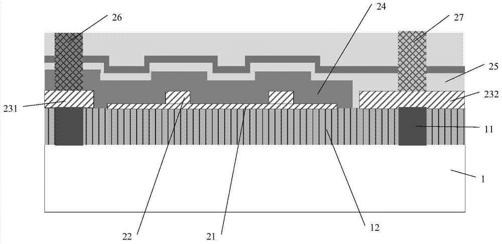
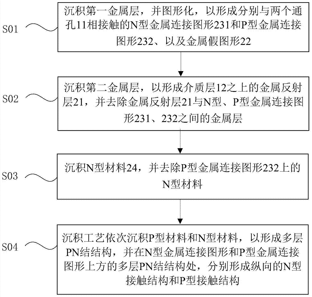
[0032] see figure 1 , the pixel structure of the CMOS image sensor of this embodiment, which is made on the top layer of the reading circuit 1, the top layer of the reading circuit 1 includes a dielectric layer 12 and a through hole 11 on both sides of the dielectric layer 12, the pixel Structures include:
[0033] The metal reflective layer 21 is located on the dielectric layer 12;
[0034] The metal dummy pattern 22 is located on the metal reflective layer 21;
[0035] Metal connection patterns, including N-type metal connection patterns 231 and P-type metal connection patterns 232 respectively located on the two through holes 11;
[0036] A multi-layer PN junction structure, where P-type material 25 and N-type material 24 are staggered and superimposed on the metal reflective layer 21, the metal dummy pattern 22 and the metal connection pattern;
[0037] The contact structure includes a vertical N-type contact structure 26 located on the N-type metal connection pattern 2...
PUM
 Abstract
Description
Claims
Application Information