Optoelectronic module and method for producing an optoelectronic module

An optoelectronic module, conductivity technology, applied in circuits, electrical components, electrical solid devices, etc., can solve problems such as unfavorable arrangement of multiple semiconductor chips

Active Publication Date: 2015-02-18
OSRAM OPTO SEMICONDUCTORS GMBH
View PDF7 Cites 0 Cited by
  • Summary
  • Abstract
  • Description
  • Claims
  • Application Information

AI Technical Summary

Problems solved by technology

In addition, however, the arrangement of the plurality of semiconductor chips required for this may be disadvantageous for reasons of routability and contactability

Method used


Image

  • Optoelectronic module and method for producing an optoelectronic module
  • Optoelectronic module and method for producing an optoelectronic module
  • Optoelectronic module and method for producing an optoelectronic module

Examples


Embodiment Construction

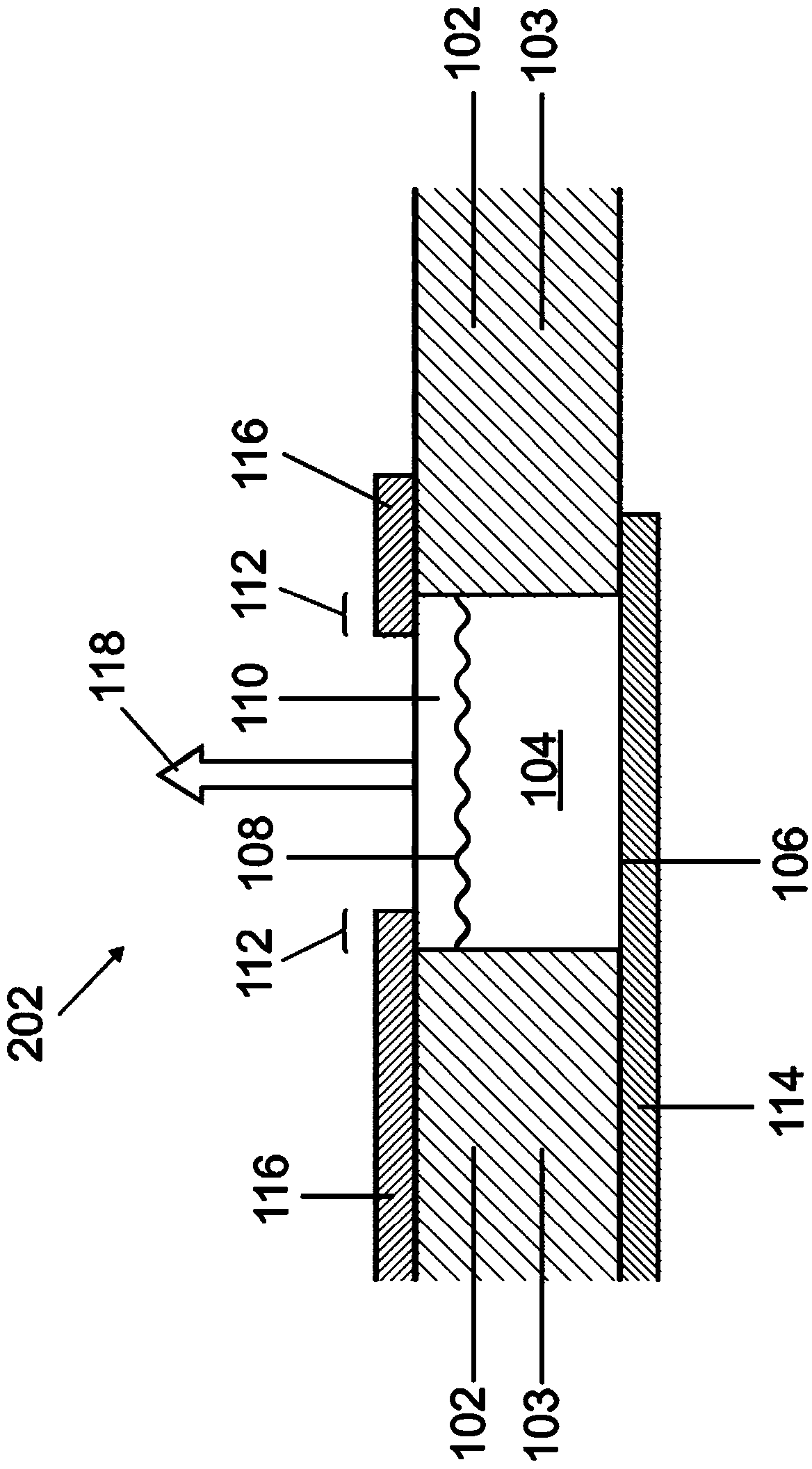
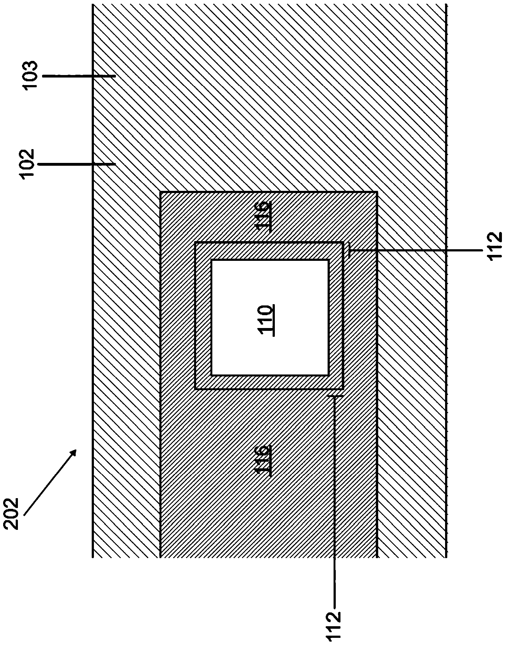
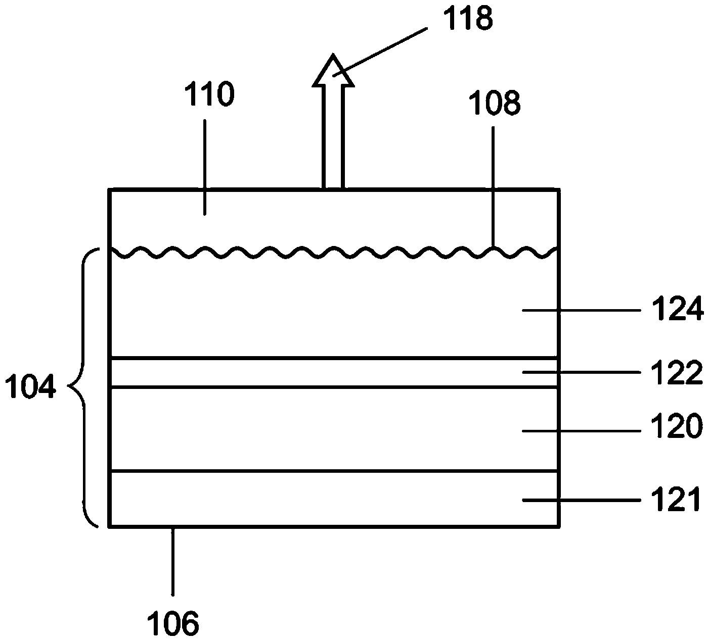
[0134] Figure 1a A sectional view of a first exemplary embodiment of an optoelectronic module 202 according to the invention is shown. Module 202 has a semiconductor chip 104 for emitting electromagnetic radiation 118 . The semiconductor chip 104 has a plurality of epitaxial layer sequences (in Figure 1a not shown, see figure 2 and 3). The semiconductor chip has an emission surface 108 , which is defined as the surface of the epitaxial layer on which electromagnetic radiation 118 emerges from the semiconductor chip 104 . Radiation surface 108 has outcoupling structures (shown as corrugated lines) which increase the efficiency with which electromagnetic radiation 118 is coupled out of semiconductor chip 104 via radiation surface 108 . A first contact, which is formed as a transparent contact layer 110 , is arranged on the emission surface 108 . Transparent currently means that electromagnetic radiation in the visible spectral range passes through the contact layer 110 wi...


PUM


Abstract

An optoelectronic module (202, 204, 206, 208, 210, 212, 214, 216) has at least one semiconductor chip (104) for emitting electromagnetic radiation (118). The semiconductor chip (104) has a layer having a first conductivity (120), in particular a p-conductivity, a layer having a second conductivity (124), in particular an n-conductivity, a radiation surface (108) and a contact surface (106) which lies opposite the radiation surface (108). A contact (110, 117) is attached to the radiation surface (108). A frame (103) made of a potting compound (102) laterally encloses the semiconductor chip (104) in at least some regions such that the radiation surface (108) and the contact surface (106) are substantially free of the potting compound (102). A first contact structure (114) is arranged in at least some regions on the frame (103) and in at least some regions on the contact surface (106) and can be used for electrically contacting the layer having a first conductivity (120). A second contact structure (116, 138) is arranged in at least some regions on the frame (103) and in at least some regions on the contact (110, 117) of the radiation surface (108) and can be used for electrically contacting the layer having a second conductivity (124).

Description

technical field [0001] The invention relates to an optoelectronic module and a method for producing an optoelectronic module. Background technique [0002] The optoelectronic module can have a plurality of semiconductor chips which are arranged on a carrier. A possible goal could be to provide an area lighting device with uniform brightness. In addition, however, the arrangement of the plurality of semiconductor chips required for this may be disadvantageous for reasons of routability and contactability. Contents of the invention [0003] It is an object of the present invention to provide an optoelectronic module and a method for producing an optoelectronic module which are particularly cost-effective. [0004] An optoelectronic module is proposed having at least one semiconductor chip for emitting electromagnetic radiation. The semiconductor chip has: a layer of first conductivity, in particular of p-type conductivity; a layer of second conductivity, in particular of ...

Claims


Application Information

Patent Timeline
Patent Type & Authority Applications(China)
IPC IPC(8): H01L33/62
CPCH01L2924/0002H01L33/62H01L2933/0066H01L25/0753H01L33/54H01L2933/0033H01L2924/00H01L33/58H01L33/64H01L2933/0075H01L2933/0091
Inventor 斯特凡·伊莱克
Owner OSRAM OPTO SEMICONDUCTORS GMBH
Why Eureka
Try Eureka