Sensor based on Fano resonance characteristics of dielectric nanostructure
A technology with nanostructure and resonance characteristics, applied in the field of optical sensors, to achieve the effect of enhancing interaction and improving sensitivity
- Summary
- Abstract
- Description
- Claims
- Application Information
AI Technical Summary
Problems solved by technology
Method used
Image
Examples
Embodiment Construction
[0027] The embodiment of the present invention provides three kinds of sensors based on the Fano resonance characteristics of silicon nanostructures, but the present invention is not limited to the dielectric material defined in this embodiment.
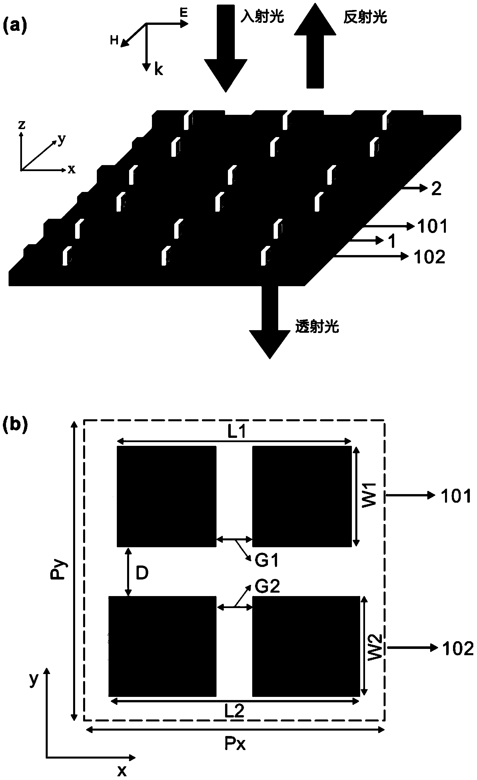
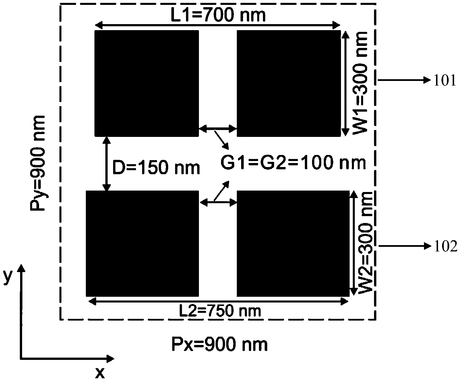
[0028] figure 1 (a) is a schematic diagram of the structure of the dielectric nanostructure array and the sensor of the present invention. Asymmetrical silicon nano-stripe pairs 1 are arranged in a uniform array on the transparent silica glass substrate 2. The silicon nano-stripe pairs 1 are composed of the first nano-stripe 101 and the second nano-stripe 102 arranged in parallel, each There is a nano groove in the middle part of the nano strip, and the depth of the groove is the same as the thickness of the nano strip. The external medium to be detected is surrounded by the silicon nano-strips, including the gaps between the nano-strips, the openings in the middle of the nano-strips, and around the upper surface of the nano-strips. It ...
PUM
| Property | Measurement | Unit |
|---|---|---|
| Length | aaaaa | aaaaa |
| Width | aaaaa | aaaaa |
| Thickness | aaaaa | aaaaa |
Abstract
Description
Claims
Application Information


