Nonvolatile memory with low power consumption and low erasing voltage based on standard technology

A non-volatile, low-power technology, applied in the field of microelectronics, can solve the problem of high power consumption, and achieve the effect of reducing high voltage, reducing technology development cycle, and high reliability

Active Publication Date: 2015-03-04
NAT UNIV OF DEFENSE TECH
View PDF9 Cites 2 Cited by
  • Summary
  • Abstract
  • Description
  • Claims
  • Application Information

AI Technical Summary

Problems solved by technology

[0005] The purpose of the present invention is to provide a non-volatile memory with low power consumption and low erasing voltage based on a standard process to solve the above-mentioned deficiencies in the prior art. Its programming and erasing operations are all completed using the FN tunneling effect. Solve the problem of high power consumption; use the pseudo-differential memory cell structure, output differential signals, high reliability, and help to use the differential structure of the sensitive amplifier to improve the read speed; the programming and erasing process requires only a low Voltage (about half of the normal high voltage) can be realized, so the high voltage generation circuit can be simplified

Method used


Image

  • Nonvolatile memory with low power consumption and low erasing voltage based on standard technology
  • Nonvolatile memory with low power consumption and low erasing voltage based on standard technology
  • Nonvolatile memory with low power consumption and low erasing voltage based on standard technology

Examples


Embodiment Construction

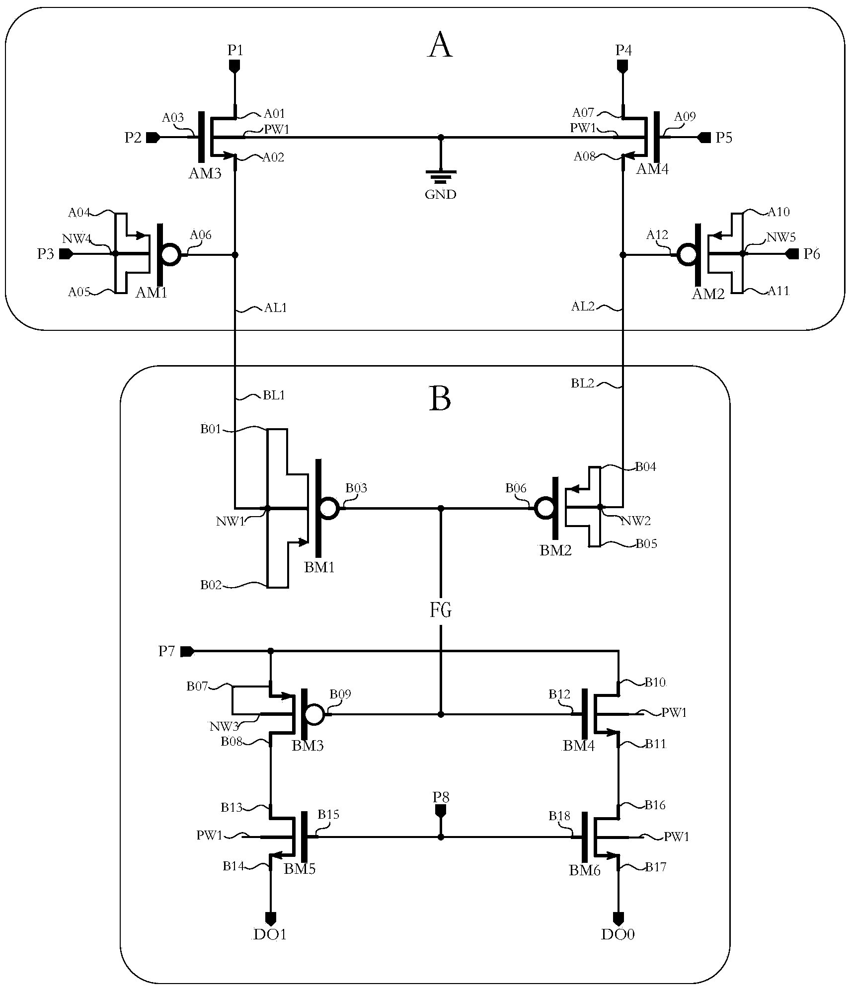
[0028] The nonvolatile memory with low power consumption and low erase / write voltage based on the standard process according to the embodiment of the present invention will be described in detail below with reference to the accompanying drawings.

[0029] refer to Figure 6 , the present invention is made up of exactly the same storage unit, and the storage unit of present embodiment is 16, and namely storage capacity is 16 bits, but is not limited to 16 bits, and actual storage capacity can be increased according to demand, and can utilize block storage array to increase storage capacity. From Figure 6It can be seen that in each row, the first ports P1 of all storage units are connected together; all the second ports P2 are connected together; all the third ports P3 are connected together; all the eighth ports P8 are connected in Together. In each column, all fourth ports P4 are connected together; all fifth ports P5 are connected together; all sixth ports P6 are connecte...


PUM


Abstract

The invention discloses a nonvolatile memory with low power consumption and low erasing voltage based on a standard technology. The programming and erasing operations of the nonvolatile memory are completed by utilizing an FN (Fowler-Nordheim) tunneling effect, the problem of high power consumption is solved, and the area is reduced. The nonvolatile memory comprises a plurality of memory units, wherein each memory unit consists of a module A and a module B; each module A comprises four transistors, namely a first voltage increasing tube AM1, a second voltage increasing tube AM2, a first charging tube AM3 and a second charging tube AM4; each module B comprises a control tube BM1, a tunneling tube BM2, a first reading tube BM3, a second reading tube BM4, a first selecting tube BM5 and a second selecting tube BM6; all the transistors adopt single polysilicon gate structures and gate oxide layers with the same thickness; the memory units are compatible with a standard CMOS technology. According to the invention, the application cost is reduced, the technical development period is reduced, the reading speed is higher, and the reliability is high.

Description

technical field [0001] The invention belongs to the technical field of microelectronics, relates to a storage technology of a semiconductor integrated circuit, in particular to a nonvolatile memory with low power consumption and low erasing voltage based on a standard process. Background technique [0002] Many integrated electronic devices require some amount of non-volatile memory. Usually non-volatile memory is used as an independent memory outside the chip or as a memory in the tag chip, mainly to store some control programs, processing instructions or items related to the chip for a long time without power supply. information and more. [0003] Several types of non-volatile memory commonly used at present mainly include erasable programmable read-only memory EPROM, electrically erasable programmable read-only memory EEPROM and flash memory Flash Memory. In addition, there are ferroelectric memory FeRAM, magnetic random access memory MRAM and phase change memory OUM an...

Claims


Application Information

Patent Timeline
Patent Type & Authority Applications(China)
IPC IPC(8): G11C16/10G11C16/14
Inventor 李建成李文晓李聪尚靖王震吴建飞王宏义谷晓忱李松亭
Owner NAT UNIV OF DEFENSE TECH
Why Eureka
Try Eureka