SOI (Silicon On Insulator) NMOS (N-channel Metal Oxide Semiconductor) device and manufacturing method for improving ESD (Electronic Static Discharge) protection capability

A technology of ESD protection and manufacturing method, applied in semiconductor/solid-state device manufacturing, semiconductor devices, electrical components, etc., to achieve the effect of promoting uniform opening, increasing reaction speed, and improving ESD protection ability

Inactive Publication Date: 2015-03-04
SHANGHAI HUALI MICROELECTRONICS CORP
View PDF3 Cites 3 Cited by
  • Summary
  • Abstract
  • Description
  • Claims
  • Application Information

AI Technical Summary

Problems solved by technology

However, since the drain of the SOI NMOS device is completely implanted with N+, there is no room for ESD implantation below the drain. Therefore, the above-mentioned existing method of ESD implantation in the drain region is no longer applicable, and other new technologies must be used to improve ESD protection capability of SOI NMOS devices

Method used


Image

  • SOI (Silicon On Insulator) NMOS (N-channel Metal Oxide Semiconductor) device and manufacturing method for improving ESD (Electronic Static Discharge) protection capability
  • SOI (Silicon On Insulator) NMOS (N-channel Metal Oxide Semiconductor) device and manufacturing method for improving ESD (Electronic Static Discharge) protection capability
  • SOI (Silicon On Insulator) NMOS (N-channel Metal Oxide Semiconductor) device and manufacturing method for improving ESD (Electronic Static Discharge) protection capability

Examples


Embodiment Construction

[0029] The specific embodiment of the present invention will be further described in detail below in conjunction with the accompanying drawings.

[0030] It should be noted that, in the following specific embodiments, when describing the embodiments of the present invention in detail, in order to clearly show the structure of the present invention for the convenience of description, the structures in the drawings are not drawn according to the general scale, and are drawn Partial magnification, deformation and simplification are included, therefore, it should be avoided to be interpreted as a limitation of the present invention.

[0031] In the following specific embodiments of the present invention, a method for fabricating an SOI NMOS device with improved ESD protection capability according to the present invention is described in detail.

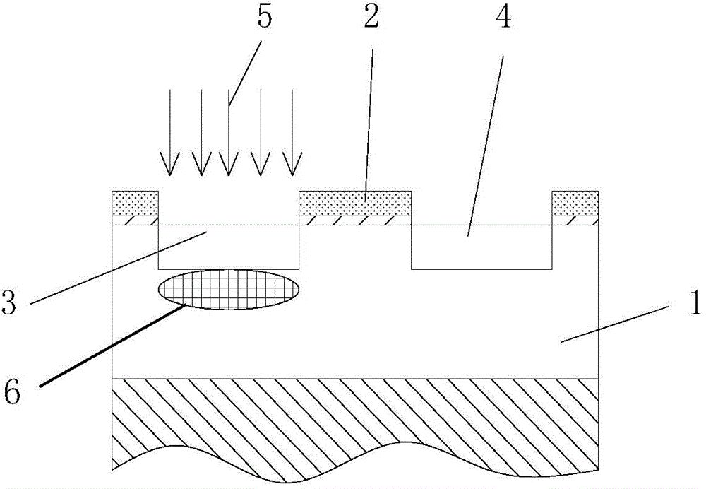
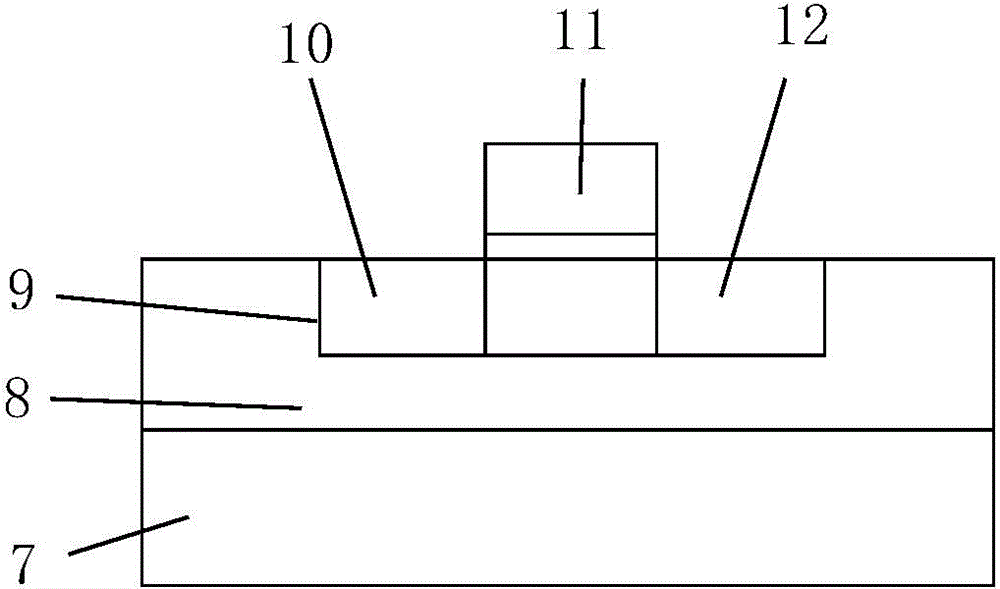
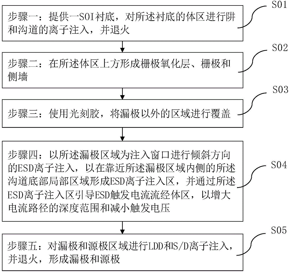
[0032] see image 3 , image 3 It is a flowchart of a SOI NMOS device manufacturing method for improving ESD protection capability of ...


PUM


Abstract

The invention discloses an SOI (Silicon On Insulator) NMOS (N-channel Metal Oxide Semiconductor) device and a manufacturing method for improving the ESD (Electronic Static Discharge) protection capability. A drain electrode area of the device serves as an implanting window to perform the ESD implanting in the inclined direction, an ESD ion implantation area is formed in the body area channel bottom local area which is close to the inner side of the drain electrode area, the ESD triggering current is guided through the ESD ion implantation area to flow through a body area so as to increase the depth range of the current path and reduce the triggering voltage, and accordingly the reaction speed of the SOI NMOS device when the ESD arrives can be improved and the improvement of the ESD protection capability of the device can be implemented.

Description

technical field [0001] The invention relates to the technical field of manufacturing semiconductor integrated circuits, and more particularly relates to an SOI NMOS device capable of improving ESD protection and a manufacturing method. Background technique [0002] As semiconductor device technology continues to enter submicron and deep submicron, the reliability of ESD (electrostatic discharge) protection devices becomes more and more important. [0003] In order to overcome the problem of decreased electrostatic discharge protection ability caused by the LDD structure, electrostatic discharge ion implantation (ESD implant) technology is used to improve the ESD protection ability of NMOS devices. The principle is to make two different NMOS devices on the same circuit , one is an NMOS device with an LDD structure for internal circuit units; the other is an NMOS device without an LDD structure for input / output ports. By adding an ESD injection layer on the NMOS device at the...

Claims


Application Information

Patent Timeline
Patent Type & Authority Applications(China)
IPC IPC(8): H01L29/78H01L21/265H01L21/336
CPCH01L29/6659H01L21/26513H01L29/66598H01L29/7833
Inventor 颜丙勇杜宏亮
Owner SHANGHAI HUALI MICROELECTRONICS CORP
Why Eureka
Try Eureka