Touch scanning circuit, touch driving circuit and touch display screen

A technology of touch scanning and circuit, which is applied in the field of touch scanning circuit, touch driving circuit and touch display screen, and can solve the problems of restricting the application of embedded technology, increasing and increasing the wiring space, etc.

Active Publication Date: 2015-03-04
BOE TECH GRP CO LTD +1
View PDF4 Cites 13 Cited by
  • Summary
  • Abstract
  • Description
  • Claims
  • Application Information

AI Technical Summary

Problems solved by technology

However, as the size of the display screen increases and the number of touch scanning lines Txn increases, the wiring for transmitting touch scanning signals to the touch scanning lin...

Method used


Image

  • Touch scanning circuit, touch driving circuit and touch display screen
  • Touch scanning circuit, touch driving circuit and touch display screen
  • Touch scanning circuit, touch driving circuit and touch display screen

Examples


example 1

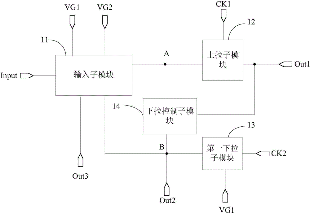
[0115] in Figure 4a In the touch scanning circuit shown, the effective pulse signal of the input signal Input is a high potential signal, the first potential is a high potential, the second potential is a low potential, the voltage of the first direct current source VG1 is a high potential, and the second direct current The voltage of source VG2 is low potential, all switching transistors are N-type transistors, and the corresponding input and output timing diagrams are as follows Figure 6a Shown. Specifically, select such as Figure 6a There are three stages of T1, T2 and T3 in the input and output timing diagram shown.

[0116] In the T1 phase, Input=1, CK1=0, and CK2=0. Since Input=1, the fourth switch transistor T4, the fifth switch transistor T5, and the sixth switch transistor T6 are turned on, the potential of the second node B is a low potential, the second output terminal Out2 outputs a low potential signal, and the third output terminal Out3 A high potential signal i...

example 2

[0124] in Figure 4b In the touch scanning circuit shown, the effective pulse signal of the input signal Input is a low potential signal, the first potential is a low potential, the second potential is a high potential, the voltage of the first DC source VG1 is a low potential, and the second DC The voltage of the source VG2 is high, and all switching transistors are P-type transistors. The corresponding input and output timing diagrams are as follows Figure 6b Shown. Specifically, select such as Figure 6b There are three stages of T1, T2 and T3 in the input and output timing diagram shown.

[0125] In the T1 phase, Input=0, CK1=1, and CK2=1. Since Input=0, the fourth switch transistor T4, the fifth switch transistor T5, and the sixth switch transistor T6 are turned on, the potential of the second node B is high, the second output terminal Out2 outputs a high potential signal, and the third output terminal Out3 A low potential signal is output, the potential of the first node ...

example 3

[0133] in Figure 5a In the touch scanning circuit shown, the effective pulse signal of the input signal Input is a high potential signal, the first potential is a high potential, the second potential is a low potential, the voltage of the first direct current source VG1 is a high potential, and the second direct current The voltage of source VG2 is low potential, all switching transistors are N-type transistors, and the corresponding input and output timing diagrams are as follows Figure 7a Shown. Specifically, select such as Figure 7a There are four stages T1, T2, T3 and T4 in the input and output timing diagram shown.

[0134] Specifically, in the T1, T2, and T3 stages, CK3=0, the twelfth switching transistor T12 is in the off state, and the specific working process of the touch scanning circuit is the same as the working process of the three stages T1, T2, and T3 in Example 1. , I won’t repeat it here.

[0135] In the T4 stage, Input=0, CK1=0, CK2=0, CK3=1. Since CK3=1, the...


PUM


Abstract

The invention discloses a touch scanning circuit, a touch driving circuit and a touch display screen. A third output end outputs a first potential signal and first and second output ends output a second potential signal under the control of an input signal of a shift register module in the touch screening circuit; the first output end outputs the first potential signal and the second and third output ends output the second potential signal under the control of a first clock signal; the second output end outputs the first potential signal and the first and third output ends output the second potential signal under the control of a second clock signal; a signal of a first reference signal end is provided for a scanning signal output end by an output module when a signal of a first input end is the first potential signal, and a signal of a second reference signal end is provided for a scanning signal output end when the signal of the second or third input end is the first potential signal. Through mutual match of the two modules, the touch scanning circuit of a simple structure is realized.

Description

Technical field [0001] The invention relates to the technical field of touch control, in particular to a touch scanning circuit, a touch driving circuit and a touch display screen. Background technique [0002] With the rapid development of display technology, touch screen panels have gradually spread throughout people's lives. At present, touch screens can be divided into: Add on Mode Touch Panel, On Cell Touch Panel, and In Cell Touch Panel according to their composition structure. Among them, the plug-in touch screen is produced separately from the touch screen and the display screen, and then bonded together to become a display screen with touch function. The plug-in touch screen has disadvantages such as high production cost, low light transmittance, and thicker modules. The in-cell touch screen embeds the touch electrodes of the touch screen inside the display screen, which can reduce the overall thickness of the module and greatly reduce the production cost of the touch s...

Claims


Application Information

Patent Timeline
IPC IPC(8): H03M11/20
Inventor 韦东梅邓银谭文
Owner BOE TECH GRP CO LTD
Why Eureka
Try Eureka