Design method for rapidly changing electrical properties of through hole in PCB (Printed Circuit Board)

A technology of electrical properties and design methods, applied in the directions of calculation, electrical digital data processing, special data processing applications, etc., can solve the problems of wasting the working time of wiring design engineers and affecting the efficiency of via design engineering, so as to reduce risks and operations time and work efficiency

Active Publication Date: 2015-03-11
LANGCHAO ELECTRONIC INFORMATION IND CO LTD
View PDF3 Cites 7 Cited by
  • Summary
  • Abstract
  • Description
  • Claims
  • Application Information

AI Technical Summary

Problems solved by technology

It wastes the working time of wiring design engineers and seriously affects the efficiency of via design engineering

Method used


Image

  • Design method for rapidly changing electrical properties of through hole in PCB (Printed Circuit Board)

Examples


Embodiment 1

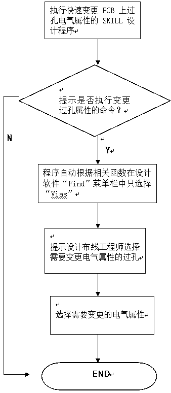
[0011] The design method for quickly changing the electrical properties of the via holes on the PCB described in this embodiment is completed using the CADENCE ALLEGRO wiring design software and the CADENCE AXLSKILL development language. By using the CADENCE AXLSKILL language to write the Skill program, put the Skill program into the wiring tool installation In the file, execute the Skill program, and the wiring designer selects whether to change the electrical properties of the vias in the pop-up menu, selects the vias that need to be changed, and specifies the electrical properties to be changed. This design method is very simple and convenient to operate, which greatly improves the work efficiency of the wiring design engineer, and at the same time prevents the wiring design engineer from repeating some very boring work.

[0012] attached figure 1 For the implementation flowchart of the design method described in this embodiment, after the execution program starts, accordin...


PUM


Abstract

The invention discloses a design method for rapidly changing the electrical properties of a through hole in a PCB (Printed Circuit Board). The design method disclosed by the invention comprises the following steps: writing an Skill program by using CADENCEAXLSKILL language, putting the written Skill program into a wiring tool installation file, executing the Skill program, selecting the through hole, the electrical properties of which need to be changed, and simultaneously, appointing names of the electrical properties to be changed, so that the properties of the selected through hole are changed into required electrical properties. Original artificial and mechanical fussy operation is changed into very simple automatic one-key operation; therefore, the working efficiency of wiring design engineers is increased to a great extent; and simultaneously, the design risk is also greatly reduced.

Description

technical field [0001] The invention relates to PCB design and production, in particular to a design method for quickly changing the electrical properties of via holes on the PCB. Background technique [0002] Components, vias, lines, copper foil and boards are several important factors that make up a PCB board. In PCB design, adding vias is a very important job. It can be said that in any PCB, vias with different electrical properties need to be added for layer change of signals, current transmission of power supply, return flow of reference GND, etc. The design of via holes is becoming more and more important in PCB design. The high-speed signal layer change processing and the operation of adding ground holes when changing layers, the power supply layer change operation, and the via hole processing of the signal FANOUT in the CPU are all very important in design engineering. Work. [0003] In the design, the change of the electrical properties of vias is a headache for ...

Claims


Application Information

Patent Timeline
IPC IPC(8): G06F17/50
Inventor 赵亚民范晓丽
Owner LANGCHAO ELECTRONIC INFORMATION IND CO LTD
Why Eureka
Try Eureka