
Pixel unit, pixel structure and manufacturing method thereof

A pixel unit and pixel structure technology, applied in the field of OLED, can solve the problems of white dots turning into yellow dots, affecting display effect and user experience, losing dot matrix effect, etc.

Active Publication Date: 2015-03-11
KUNSHAN GO VISIONOX OPTO ELECTRONICS CO LTD
View PDF5 Cites 16 Cited by
  • Summary
  • Abstract
  • Description
  • Claims
  • Application Information

AI Technical Summary

Problems solved by technology

The disadvantages of this scheme are: (1) When displaying vertical lines, the vertical alternate arrangement of RB pixels at the black and white borderline will lead to "color fringe" phenomenon; (2) When displaying dot matrix, all blue pixels should be extinguished , at this time each pixel has lost its neighbors and cannot be shared, causing the white dot to turn into a yellow dot. If you want to avoid this phenomenon, you need to light up the blue again, and the dot matrix effect will be lost. (3) When the diagonal line is displayed, The red pixels on the edge cause serious aliasing. (4) In order to avoid the influence of tolerance during the production process, sufficient gaps (gap) need to be reserved between adjacent pixel units to affect the pixel density.
Its defect is that vertical pixels are arranged in a staggered manner, resulting in a strong sense of jaggedness, graininess and glitches when displaying the edges of oblique lines, horizontal lines and vertical lines, which greatly affects the display effect and user experience.

Method used


Image

  • Pixel unit, pixel structure and manufacturing method thereof
  • Pixel unit, pixel structure and manufacturing method thereof
  • Pixel unit, pixel structure and manufacturing method thereof

Examples


Embodiment Construction

[0029] In order to facilitate the understanding of the present invention, the present invention will be described more fully below with reference to the associated drawings. Preferred embodiments of the invention are shown in the accompanying drawings. However, the present invention can be embodied in many different forms and is not limited to the embodiments described herein. On the contrary, these embodiments are provided to make the understanding of the disclosure of the present invention more thorough and comprehensive.

[0030] It should be noted that when an element is referred to as being “fixed” to another element, it can be directly on the other element or there can also be an intervening element. When an element is referred to as being "connected to" another element, it can be directly connected to the other element or intervening elements may also be present. In contrast, when an element is referred to as being "directly on" another element, there are no interveni...


PUM


Abstract

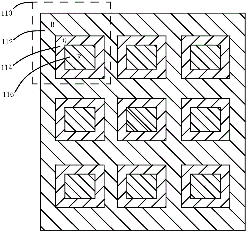
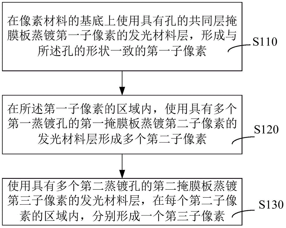
The invention discloses a pixel unit and a pixel structure. The pixel unit comprises first sub pixels, second sub pixels and third sub pixels. The first sub pixels surround the second sub pixels, and the second sub pixels surround the third sub pixels. The sub pixels are embedded and match with each others; when the pixel units are arrayed on one transverse line or vertical line, the sub pixels are not staggered, and jagged sense and burr sense are avoided. The invention further provides a pixel structure manufacture method, additional reserved gaps are omitted during pixel evaporation, process difficulty can be lowered, and process qualification rate can be increased.

Description

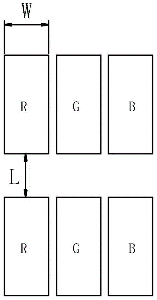
technical field [0001] The invention relates to the technical field of OLEDs, in particular to a pixel unit of an OLED display screen, a pixel structure and a manufacturing method thereof. Background technique [0002] The OLED (Organic Light-Emitting Diode, Organic Light-Emitting Diode, Organic Light-Emitting Diode) colorization technology that is relatively mature and has been successfully mass-produced at present is OLED evaporation technology, which adopts the traditional RGB (red, green and blue) stripe arrangement for OLED evaporation, but is affected Limited to the precision of the evaporation mask (mask) and the precision of the evaporation process, it is very difficult to realize high-resolution OLED products by evaporation. [0003] At present, there are two main methods for OLED evaporation. One is Slit (slot) type: see figure 1 , using this method, between the upper and lower rows of RGB, the corresponding sub-pixels such as R sub-pixels will be connected toget...

Claims


Application Information

Patent Timeline
IPC IPC(8): H01L27/32H01L51/56
Inventor 刘敏魏朝刚
Owner KUNSHAN GO VISIONOX OPTO ELECTRONICS CO LTD
Learn More