Technological mapping method and integrated circuit for optimizing register control signal

A control signal and process mapping technology, applied in the field of process mapping, can solve the problems of scattered control signals, loose layout results, and large complexity, and achieves the effect of optimizing register control signals and improving the success rate.

Active Publication Date: 2015-03-18
CAPITAL MICROELECTRONICS
View PDF5 Cites 8 Cited by
  • Summary
  • Abstract
  • Description
  • Claims
  • Application Information

AI Technical Summary

Problems solved by technology

[0004] The object of the present invention is to provide a process mapping method and an integrated circuit that reduce the number of independent control signals in the logic synthesis stage to improve the success rate of layou

Method used


Image

  • Technological mapping method and integrated circuit for optimizing register control signal
  • Technological mapping method and integrated circuit for optimizing register control signal
  • Technological mapping method and integrated circuit for optimizing register control signal

Examples


Embodiment Construction

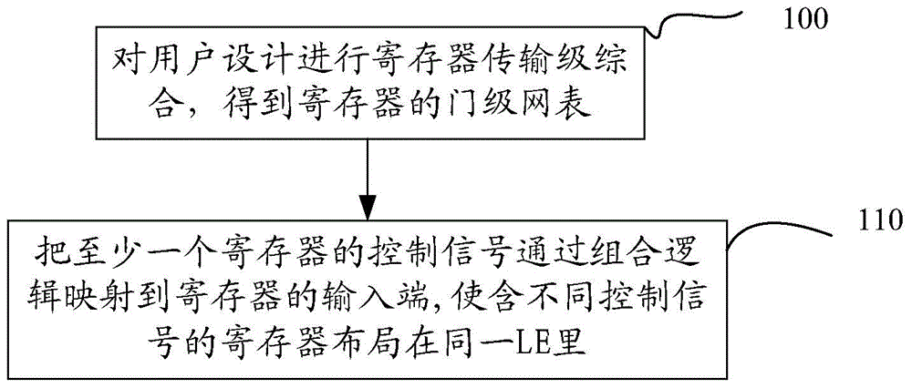
[0017] figure 1 It is a flowchart of a process mapping method for optimizing register control signals in the present invention. The method includes the following steps:

[0018] In step 100, register-transfer-level synthesis is performed on the user design to obtain a gate-level netlist of registers. RTL (Register-transfer Level), that is, the register transfer level, there is a direct mapping relationship between the statements in the RTL model writing and the actual register structure model, and the register transfer level synthesis is to map the RTL writing to specific devices to achieve equivalence The function of the gate-level netlist is to realize the function of RTL under the specific process (such as smic0.13um logic G) of specific devices (such as standard cells). For example, in RTL, Y=A+C; then in the gate-level netlist, it will become: there is a standard unit OR2X2 under smic0.13um logic G, its input is A, C, and its output is Y.

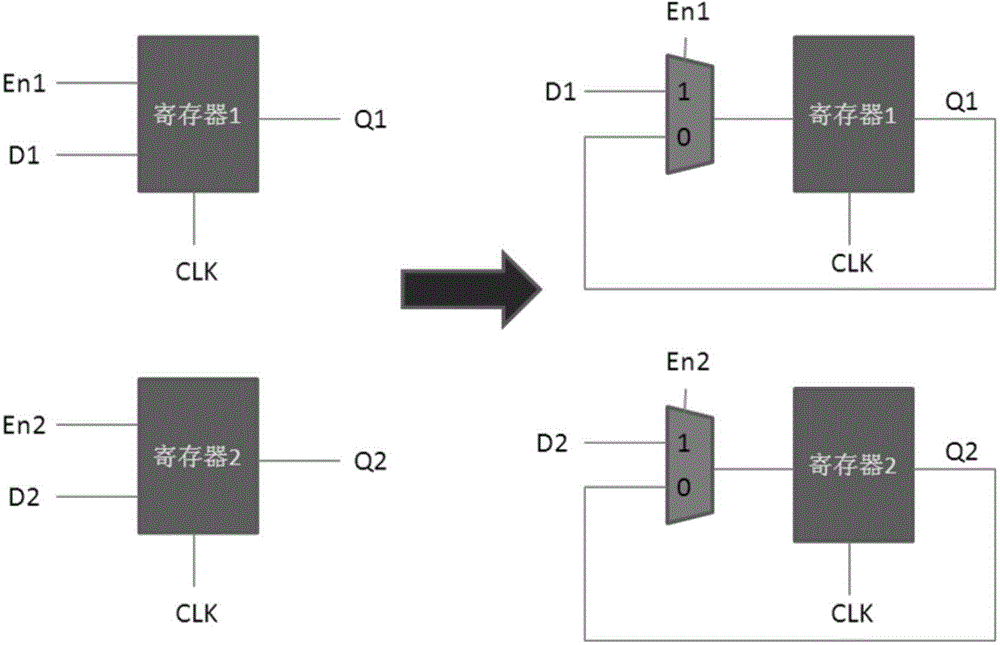
[0019] In step 101, the cont...


PUM


Abstract

The invention relates to a technological mapping method and an integrated circuit for optimizing a register control signal. The method comprises the following steps of: performing register transport level integration on a user design to obtain a gate level net list of a register; mapping a control signal of at least one register to an input end of the register by virtue of combined logic mapping, so that the register with different control signals is arranged in the same LE. The technological mapping method can be used for enabling the register with multiple independent control signals to arrange in the same PLB, so that the quantity of the independent control signals is lowered, and the wiring success rate is increased.

Description

technical field [0001] The present invention relates to FPGA, in particular to a process mapping in FPGA hardware architecture. Background technique [0002] In many FPGA (Field-Programmable Gate Array, Field Programmable Gate Array) hardware architectures, a group of registers in a PLB (Programmable Logic Block, or programmable logic module) usually share the same control signal (so that Can / reset / set), so registers with the same control signal must be placed in the same PLB when layout and routing. For large designs with more registers with independent control signals, they must be placed Distributed to different PLBs, so that the result of layout is quite loose, which will increase the complexity of wiring and reduce the success rate of wiring. Even designs with too many independent control signals fail at the layout stage. [0003] It is urgent to design a method to reduce the number of independent control signals in the logic synthesis stage to improve the success rat...

Claims


Application Information

Patent Timeline
IPC IPC(8): G06F17/50H03K19/00
Inventor 耿嘉樊平刘明
Owner CAPITAL MICROELECTRONICS
Why Eureka
Try Eureka