Super junction device and manufacturing method thereof

A super junction and device technology, used in semiconductor/solid-state device manufacturing, semiconductor devices, electrical components, etc., can solve the problems of hard reverse recovery characteristics of diodes, severe reverse recovery fluctuations, and changes in device recovery currents. Optimal balance of on-resistance, reduction of recovery current shock, and optimal balance of withstand current shock

Active Publication Date: 2015-03-18
SHANGHAI HUAHONG GRACE SEMICON MFG CORP
View PDF5 Cites 0 Cited by
  • Summary
  • Abstract
  • Description
  • Claims
  • Application Information

AI Technical Summary

Problems solved by technology

[0004] In the super junction process, due to the use of alternate P / N thin layers, the body diode of the super junction device, that is, the diode formed between the P-type semiconductor thin layer and the N-type semiconductor thin layer, can operate at a lower reverse bias voltage such as 50 Vds will completely deplete the P-type semiconductor thin layer and the N-type semiconductor thin layer, which makes the diode have a very hard reverse recovery characteristic. This hard reverse recovery characteristic causes the recovery current of the device to change sharply. Severe fluctuations in reverse recovery cause electromagnetic noise (EMI NOISE) in the circuit, which affects the work of other devices in the circuit. In this regard, super junction devices are not as good as conventional MOSFET devices, because conventional MOSFET devices The depletion of the N-drift region always expands with the increase of the voltage (Vds), and the reverse recovery characteristic is soft

Method used


Image

  • Super junction device and manufacturing method thereof
  • Super junction device and manufacturing method thereof
  • Super junction device and manufacturing method thereof

Examples


Embodiment Construction

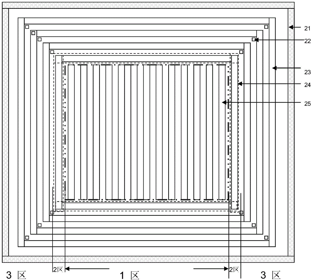
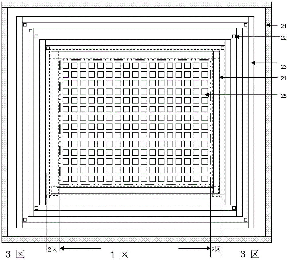
[0039] Such as figure 1 Shown is the top view of the existing super junction device Figure one . In the top view, the embodiment of the present invention can be divided into zone 1, zone 2, and zone 3. Region 1 is the middle region of the super junction device, which is the current flow region. The current flow region includes alternately arranged P-type regions 25 and N-type regions. The P-type region 25 is also the P-type region formed in the current flow region. The N-type thin layer, the N-type region is also the N-type thin layer formed in the current flow region; in the current flow region, the current will pass through the N-type region from the source to the drain through the channel, and the The P-type region 25 and the N-type region form a depletion region to withstand voltage in the reverse blocking state. Zone 2 and Zone 3 are the terminal protection structure area of ​​the super junction device. When the device is turned on, the terminal protection structure does...


PUM


Abstract

The invention discloses a super junction device. A current flowing region includes a plurality of N type thin layers and P type thin layers which are arranged alternately, wherein each N type thin layer includes a high-resistivity portion at the middle and low-resistivity portions at two sides; charges of the N type thin layers and charges of the P type thin layers are not balanced; charges of the low-resistivity portions of the N type thin layers and charges of the P type thin layers are balanced; the P type thin layers cannot perform complete horizontal depletion on the high-resistivity portions; and P wells at the tops of the N type thin layers perform gradually-expanded longitudinal depletion on the high-resistivity portions of the N type thin layers with the increase of reverse bias voltage. The invention also discloses a manufacturing method of the super junction device. With the super junction device and the manufacturing method thereof of the invention adopted, the reverse recovery characteristics of the device can be improved, and the device can have low specific on resistance.

Description

Technical field [0001] The invention relates to the field of semiconductor integrated circuit manufacturing, in particular to a super junction device; the invention also relates to a manufacturing method of a super junction device. Background technique [0002] Super junction MOSFET adopts a new withstand voltage layer structure, using a series of alternately arranged P-type semiconductor thin layers and N-type semiconductor thin layers to combine the P-type semiconductor thin layers and N-type semiconductor thin layers at a lower voltage in the off state. Type semiconductor thin layer is depleted to achieve mutual compensation of charges, so that P-type semiconductor thin layer and N-type semiconductor thin layer can achieve high breakdown voltage under high doping concentration, thereby achieving low on-resistance and high breakdown at the same time Voltage, breaking the theoretical limit of traditional power MOSFET. In the US patent US5216275, the above alternately arranged P...

Claims


Application Information

Patent Timeline
Patent Type & Authority Applications(China)
IPC IPC(8): H01L29/78H01L29/06H01L21/336
CPCH01L29/0603H01L29/0688H01L29/66227H01L29/68
Inventor 肖胜安
Owner SHANGHAI HUAHONG GRACE SEMICON MFG CORP
Why Eureka
Try Eureka